Voltage reference source with low power consumption and low temperature coefficient
A technology of low temperature coefficient, voltage reference source, used in regulating electrical variables, control/regulating systems, instruments, etc.
- Summary
- Abstract
- Description
- Claims
- Application Information
AI Technical Summary
Problems solved by technology
Method used
Image

Examples
Embodiment 1
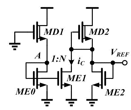
[0020] As a preferred embodiment of the present invention, the present invention discloses a voltage reference source with low power consumption and low temperature coefficient, which includes a compensation current generating circuit and a first-order temperature compensation circuit. The compensation current of the compensation current generating circuit is determined by the working Provided by the NMOS tube in the subthreshold area, the first-order temperature compensation circuit is composed of an enhanced NMOS tube and a depletion-type NMOS tube, the compensation current generation circuit is connected with the first-order compensation circuit, and the compensation current generation circuit works in the subthreshold area The depletion-type NMOS transistor introduces compensation current for the first-order compensation circuit, thereby outputting a reference voltage with a low temperature coefficient.
Embodiment 2
[0022] As the best implementation mode of the present invention, it will be specifically described below in conjunction with the accompanying drawings:
[0023] The schematic diagram of the low power consumption and low temperature coefficient voltage reference source circuit of the present invention is as follows: figure 1 shown.
[0024] Wherein, the compensation current generating circuit includes a depletion-type NMOS transistor MD1 and an enhanced-type NMOS transistor ME0 and ME1. Among them, the drain of the depletion NMOS transistor MD1 is connected to the external power supply voltage, the gate of the depletion NMOS transistor MD1 is grounded, the source of the depletion NMOS transistor MD1, the drain and the gate of the enhancement NMOS transistor ME0 are connected to the enhancement The gate of the enhanced NMOS transistor ME1 is connected as node A, the source of the enhanced NMOS transistor ME0 is grounded, the source of the enhanced NMOS transistor ME1 is ground...
PUM
 Abstract
Description
Claims
Application Information
 - R&D Engineer
- R&D Manager
- IP Professional
- Industry Leading Data Capabilities
- Powerful AI technology
- Patent DNA Extraction
Browse by: Latest US Patents, China's latest patents, Technical Efficacy Thesaurus, Application Domain, Technology Topic.
© 2024 PatSnap. All rights reserved.Legal|Privacy policy|Modern Slavery Act Transparency Statement|Sitemap