Detecting structure, forming method and detecting method

A detection structure and technology to be detected, applied in semiconductor/solid-state device testing/measurement, electrical components, electric solid-state devices, etc., can solve problems such as low detection efficiency

Active Publication Date: 2013-02-13
SEMICON MFG INT (SHANGHAI) CORP
View PDF6 Cites 12 Cited by
  • Summary
  • Abstract
  • Description
  • Claims
  • Application Information

AI Technical Summary

Problems solved by technology

However, using the detection structure, it is necessary to detect one shallow trench isolation corner area and one shallow trench isolation corner area. Each detection needs to align the detection device with the detection point corresponding to the shallow trench isolation corner area, and the detection efficiency is improved. Low

Method used


Image

  • Detecting structure, forming method and detecting method
  • Detecting structure, forming method and detecting method
  • Detecting structure, forming method and detecting method

Examples


Embodiment Construction

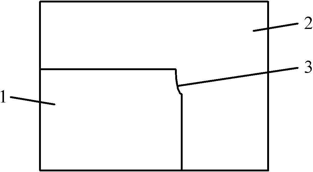
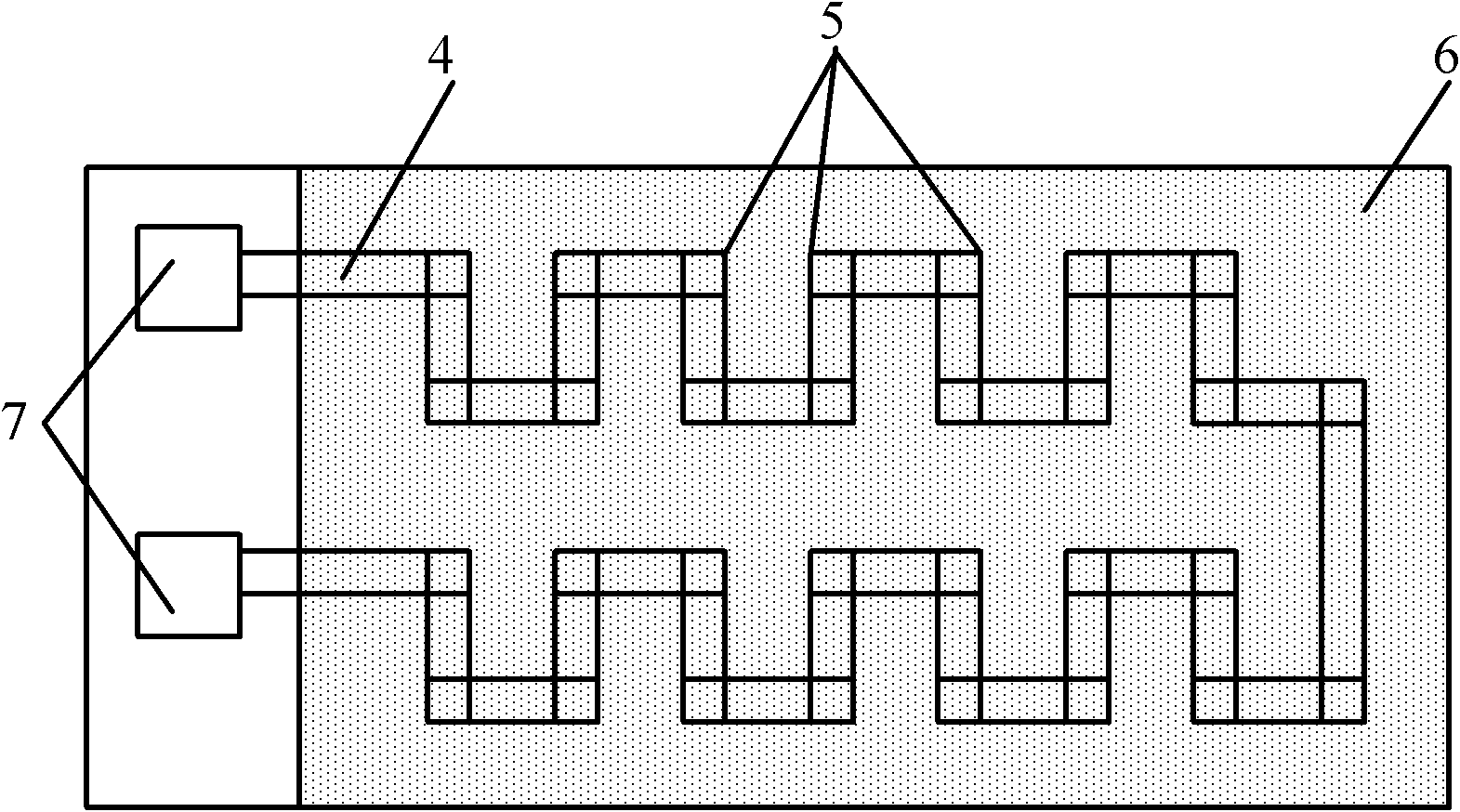
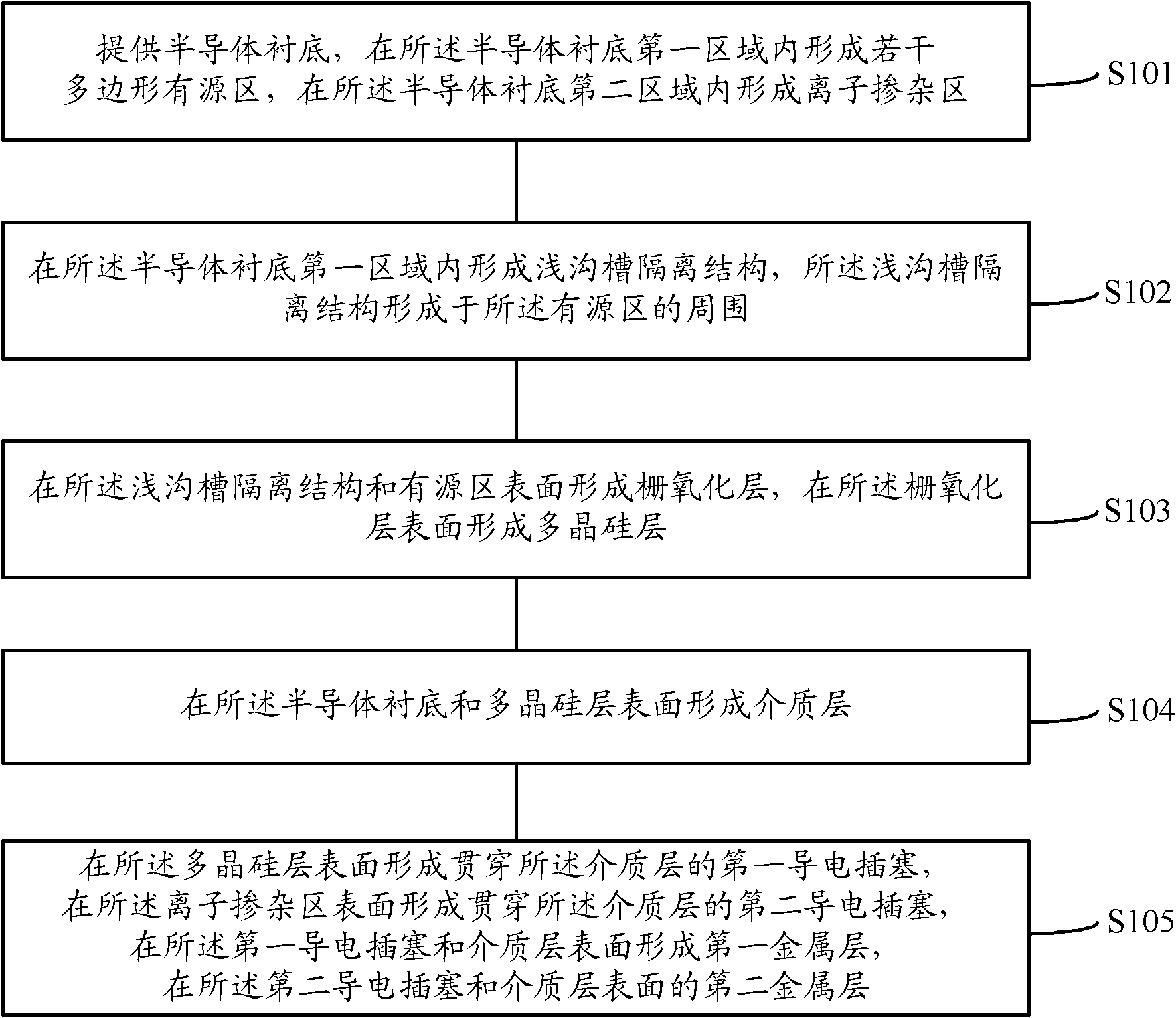
[0036] Since none of the detection structures in the prior art can quickly and effectively detect whether the corner of the active area of ​​the semiconductor device is damaged, the inventor has proposed a detection structure with high detection efficiency, a formation method and a detection method after research. The detection structure includes A number of polygonal active regions located in the semiconductor substrate, a shallow trench isolation structure is formed around the active region, a gate oxide layer and a polysilicon layer are sequentially formed on the surface of the active region and the shallow trench isolation structure, through Detecting the breakdown voltage of the gate oxide layer to determine whether the corner of the active area of ​​the detection structure is damaged, and the detection structure and the semiconductor device to be detected are formed by the same formation process, and the detection structure and the semiconductor device to be detected are f...


PUM


Abstract

The invention discloses a detecting structure, a forming method and a detecting method. The detecting structure comprises a plurality of polygon active areas, a shallow channel isolation structure, an ion mixing area, a gate oxide layer, a polycrystalline silicon layer, a dielectric layer, a first conducting plug, a second conducting plug, a first metal layer and a second metal layer, wherein the polygon active areas are positioned in a first area of a semiconductor substrate; the shallow channel isolation structure is positioned in the first area of the semiconductor substrate and is formed surrounding the active areas; the ion mixing area is positioned in a second area of the semiconductor substrate; the gate oxide layer covers the active area and the shallow channel isolation structure; the polycrystalline silicon layer is positioned on the surface of the gate oxide layer; the dielectric layer covers the semiconductor substrate and the polycrystalline silicon layer; the first conducting plug is positioned on the surface of the polycrystalline silicon layer; the second conducting plug is positioned on the surface of the ion mixing layer, and the first metal layer and the second metal layer are positioned on the surface of the dielectric layer. According to the detecting structure disclosed by the invention, whether a corner of the active area of the detecting structure is damaged or not can be detected by measuring the puncture voltage of the gate oxide layer for one time, and thus whether a corner of an active area of a to-be-detected semiconductor device is damaged or not can be judged.

Description

technical field [0001] The invention relates to a semiconductor detection process, in particular to a detection structure, a forming method and a detection method for detecting whether the corner of an active area surrounded by a shallow trench isolation structure is damaged. Background technique [0002] In the current semiconductor manufacturing process, shallow trench isolation (Shallow Trench Isolate, STI) technology has been widely used in the isolation process. Generally, a shallow trench isolation structure is formed around an active region formed in a semiconductor substrate. Currently, high-density plasma chemical vapor deposition (HDPCVD) is mostly used to form shallow trench isolation structures, and it has become the mainstream of shallow trench isolation processes due to its excellent hole filling ability, stable deposition quality and many other advantages. However, when using HDPCVD to form a shallow trench isolation structure, the shape of the corner region ...

Claims


Application Information

Patent Timeline
Patent Type & Authority Applications(China)
IPC IPC(8): H01L23/544H01L21/66
Inventor 甘正浩
Owner SEMICON MFG INT (SHANGHAI) CORP
Why Eureka
Try Eureka