LED (Light-Emitting Diode) chip and manufacturing method of LED chip

A technology of LED chip and manufacturing method, which is applied in the direction of electrical components, circuits, semiconductor devices, etc., can solve the problem that the current in the LED chip cannot be evenly distributed, and achieve good luminous efficiency, uniform light output rate, and uniform current distribution.

Inactive Publication Date: 2015-06-24
ENRAYTEK OPTOELECTRONICS
View PDF6 Cites 0 Cited by
  • Summary
  • Abstract
  • Description
  • Claims
  • Application Information

AI Technical Summary

Problems solved by technology

Further, the present invention can also solve the problem that the current in the LED chip cannot be evenly distributed

Method used


Image

  • LED (Light-Emitting Diode) chip and manufacturing method of LED chip
  • LED (Light-Emitting Diode) chip and manufacturing method of LED chip
  • LED (Light-Emitting Diode) chip and manufacturing method of LED chip

Examples


Embodiment Construction

[0032] It has been mentioned in the background technology that the traditional LED chip flip-chip manufacturing method increases the process steps and difficulty, and limits the further development of the LED chip in thickness and size. At the same time, the electrode structure of the existing LED chip can only obtain A certain degree of current expansion makes the current evenly distributed, which cannot meet the needs of further increase in chip size.

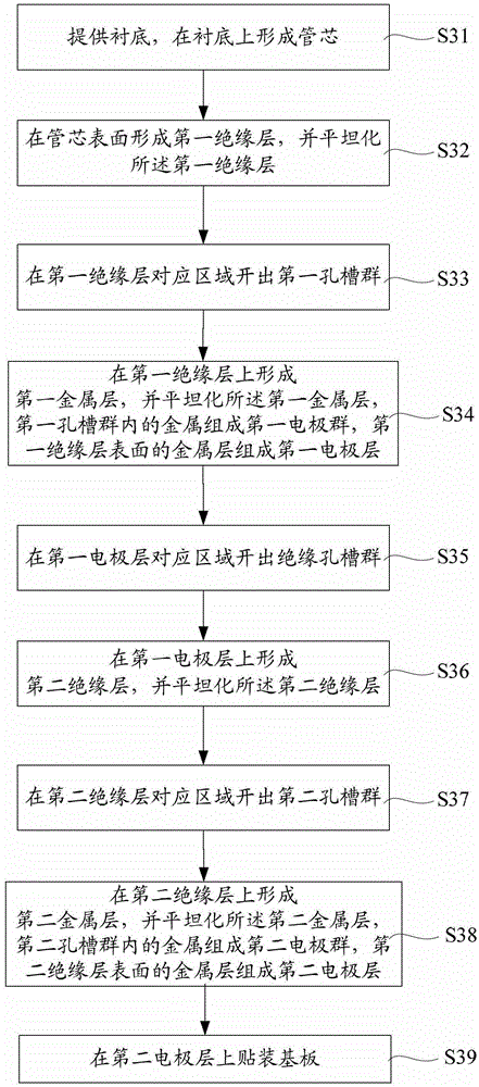
[0033] To this end, the present invention provides an LED chip and a manufacturing method thereof. The manufacturing method of the LED chip optimizes the traditional flip-chip process. Device thickness.

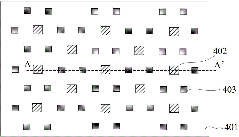
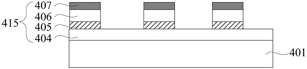
[0034] Further, the N electrode and the P electrode are separated into the first electrode group and the second electrode group, which are distributed on the corresponding area of ​​the die. Such a structure can obtain sufficient current expansion to make the current evenly distributed, so that the device can obtain good lum...


PUM


Abstract

The invention discloses an LED (Light-Emitting Diode) chip and a manufacturing method of the LED chip. The manufacturing method of the LED chip comprises the steps of continually generating structures comprising an electrode layer and an insulating layer and the like after an electrode group is generated, and two steps of the traditional flip chip process are optimized; and meanwhile, the method can effectively control the thickness of the LED chip. A pair of traditionally-arranged electrodes into a first electrode group and a second electrode group which are distributed at the corresponding regions of a pipe core; and sufficient current expansion can be obtained by the structure to uniformly distribute current, so that the uniform device has good luminous efficiency and uniform luminous rate, thereby meeting the requirement of further increasing the chip size.

Description

technical field [0001] The invention relates to the technical field of LED manufacturing, in particular to an LED chip and a manufacturing method thereof. Background technique [0002] Light Emitting Diode (LED, Light Emitting Diode) is a semiconductor solid-state light-emitting device that uses a semiconductor PN junction as a light-emitting material to convert electricity into light. When a forward voltage is applied to both ends of the semiconductor PN junction, the electrons and holes injected into the PN junction recombine, and the excess energy is released in the form of photons. LED has the advantages of long life and low power consumption. With the maturity of technology, the application fields of LED are becoming more and more diversified. The requirements for the power and brightness of LED chips are also getting higher and higher. The size of LED chips There is also further demand. [0003] In the traditional LED chip structure, the P electrode and the N electro...

Claims


Application Information

Patent Timeline
Patent Type & Authority Patents(China)
IPC IPC(8): H01L33/00H01L33/38
Inventor 毕少强
Owner ENRAYTEK OPTOELECTRONICS
Why Eureka
Try Eureka