Memristor device and manufacturing method thereof

A technology for memristors and devices, which is applied in the field of memristor devices and its preparation, can solve the problems of not finding memristors, etc., and achieve the effect of simple preparation method and compatible preparation process

Inactive Publication Date: 2013-02-13
INST OF MICROELECTRONICS CHINESE ACAD OF SCI
View PDF2 Cites 16 Cited by
  • Summary
  • Abstract
  • Description
  • Claims
  • Application Information

AI Technical Summary

Problems solved by technology

Due to the limitation of semiconductor process technology, no material was found that had obvious memristor effect.

Method used


Image

  • Memristor device and manufacturing method thereof
  • Memristor device and manufacturing method thereof
  • Memristor device and manufacturing method thereof

Examples


Embodiment Construction

[0020] In order to make the object, technical solution and advantages of the present invention clearer, the present invention will be described in further detail below in conjunction with specific embodiments and with reference to the accompanying drawings.

[0021] The drawings and their descriptions provided herein are only for illustrating embodiments of the present invention. The shapes and dimensions in the respective drawings are for schematic illustration only, and do not strictly reflect actual shapes and dimensional ratios. Furthermore, the illustrated embodiments of the invention should not be construed as limited to the specific shapes of the regions shown in the figures, the representations in which are schematic and are not intended to limit the scope of the invention.

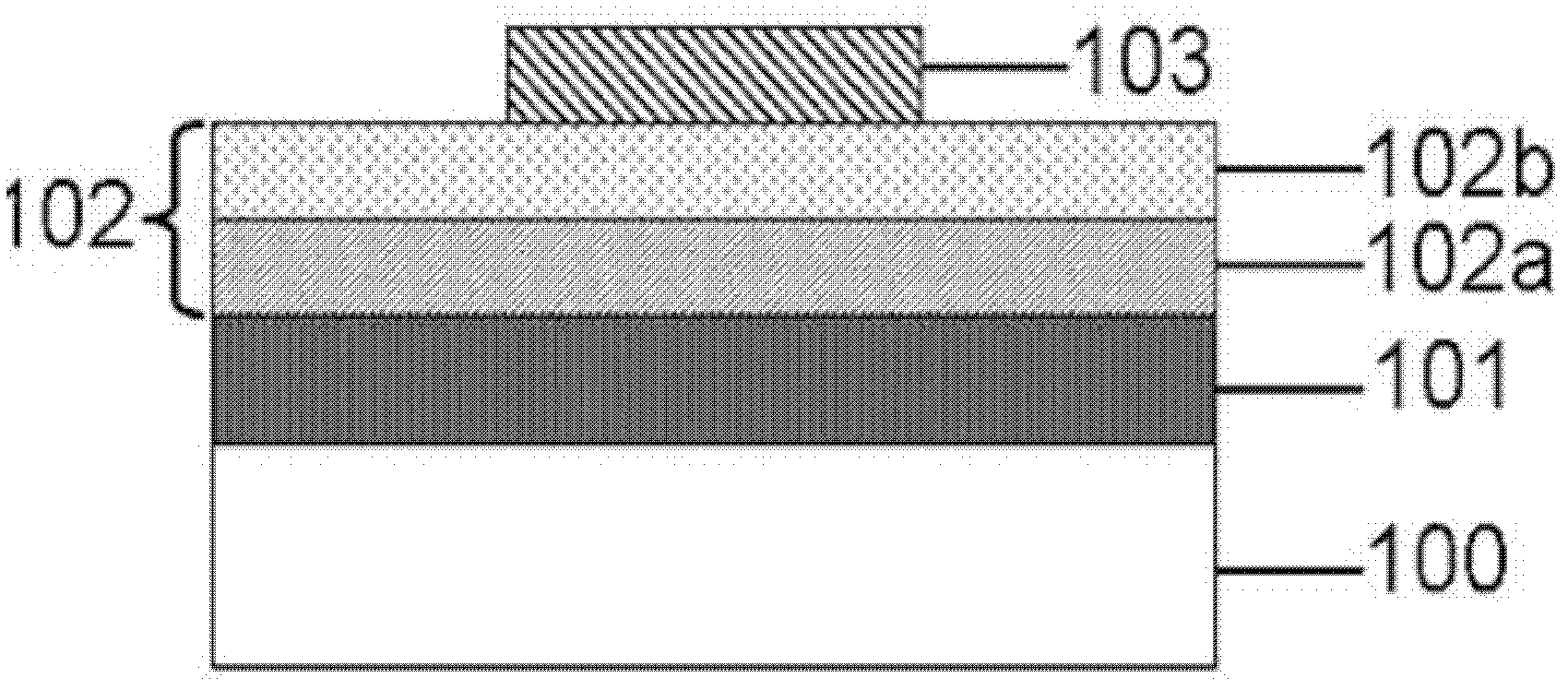
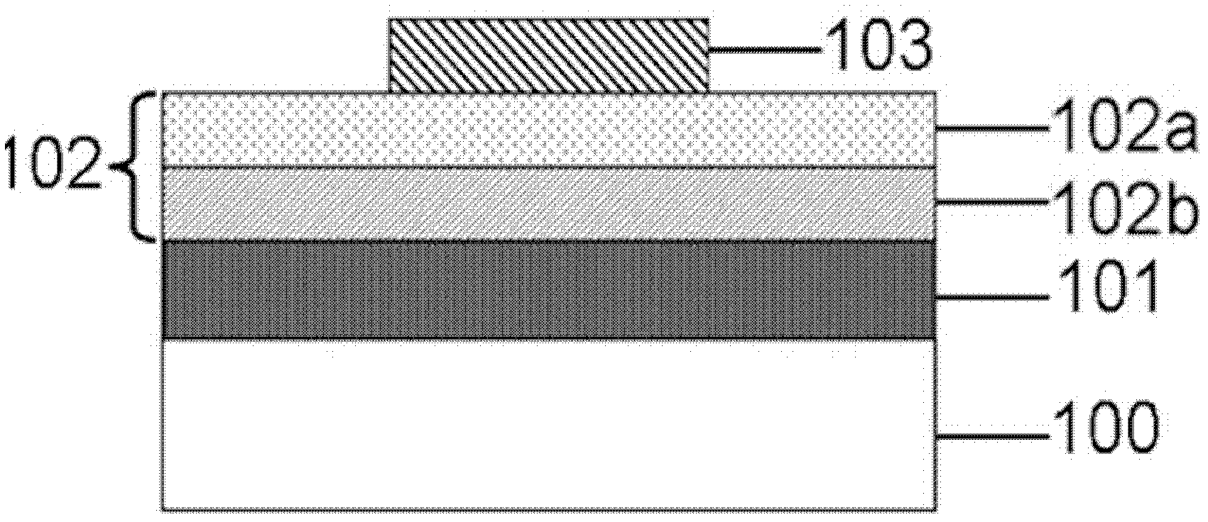
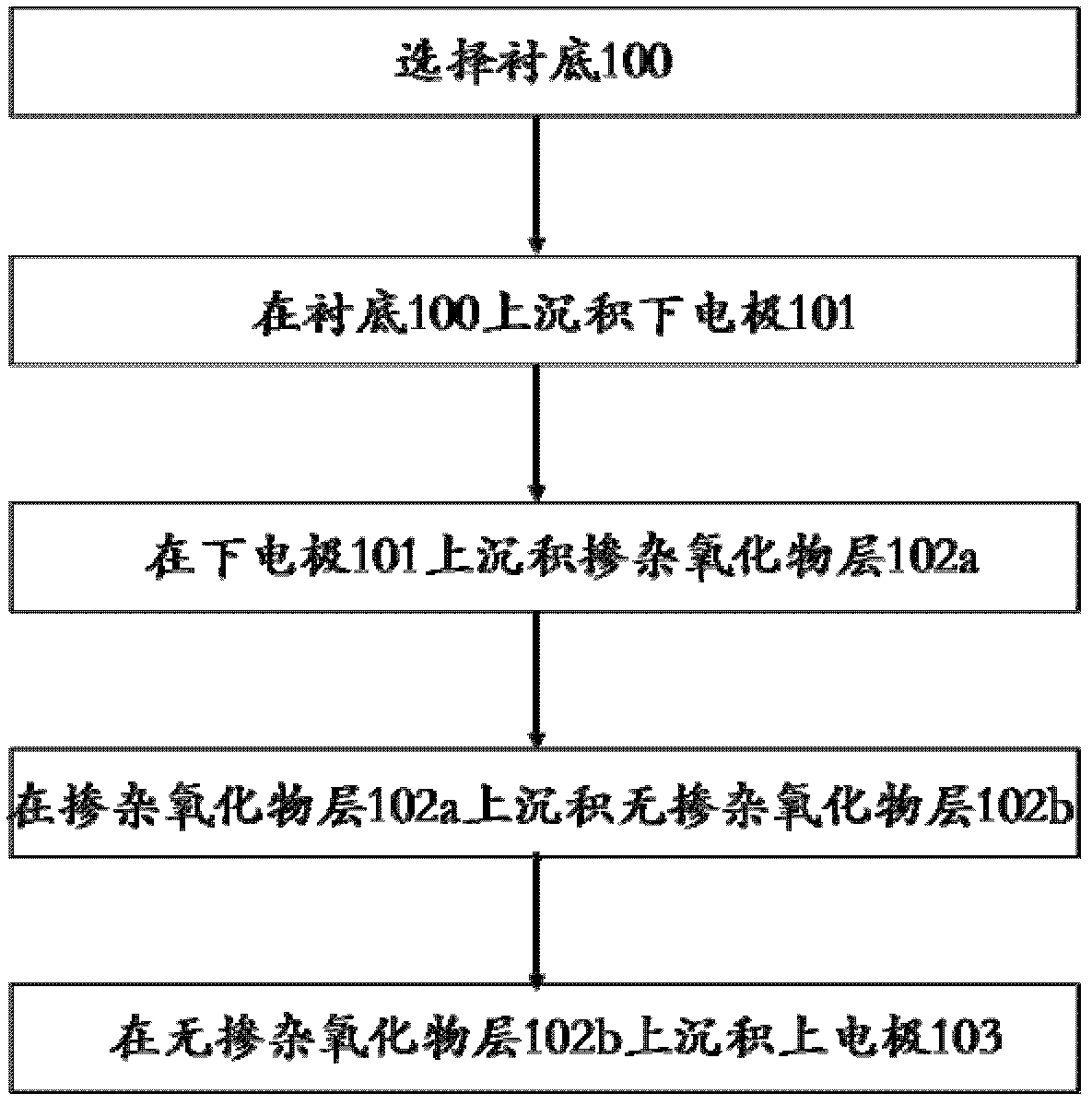
[0022] Such as figure 1 as shown, figure 1 It is a structural schematic diagram of a memristor device according to the first embodiment of the present invention, the memristor device includes: a...


PUM


Abstract

The invention discloses a memristor device and a manufacturing method thereof. The memristor device comprises a substrate, a lower electrode formed above the substrate, a memory storage layer formed above the lower electrode and an upper electrode formed above the memory storage layer, wherein the memory storage layer comprises two layers of oxide materials with different oxygen contents. The method for manufacturing the memristor device comprises the following steps of: growing a conducting material on the substrate as the lower electrode; growing the memory storage layer on the lower electrode, wherein the memory storage layer comprises two layers of oxide materials, and the oxygen contents of the two layers of oxide materials are different; and growing a conducting material on the memory storage layer as the upper electrode. The manufacturing method provided by the invention is simple, and the manufacturing technology is compatible with the traditional CMOS (Complementary Metal Oxide Semiconductors) technology and has certain application prospect in the field of memories.

Description

technical field [0001] The invention relates to the technical field of microelectronics and memory, in particular to a memristor device and a preparation method thereof. Background technique [0002] Memristors, also known as memristors, are the fourth basic passive circuit element after resistors, capacitors, and inductors have entered mainstream electronics, because they, like variable resistors, can "remember" changes in voltage by changing the voltage across them. Change the magnitude of the current passing through. Therefore, a memristor is actually a non-linear resistor with a memory function that can be used as a storage element. [0003] As early as 1971, Professor Cai Shaotang, a Chinese scientist at the University of California, Berkeley, revealed the existence of memristors from the circuit theory when studying the relationship between charge, current, voltage and magnetic flux. Due to the limitation of semiconductor process technology, no material was found tha...

Claims


Application Information

Patent Timeline
Patent Type & Authority Applications(China)
IPC IPC(8): H01L45/00
Inventor 刘明李颖弢龙世兵吕杭炳刘琦
Owner INST OF MICROELECTRONICS CHINESE ACAD OF SCI
Why Eureka
Try Eureka