A method to improve the capture rate of underetched defects

A technology for insufficient etching and defects, which is applied in the field of scanning defects, can solve the problems of reducing defect capture rate, indistinguishability, copper can not be exposed for a long time, etc., and achieve the effect of shortening the development cycle and improving the capture rate

Active Publication Date: 2015-09-30
SHANGHAI HUALI MICROELECTRONICS CORP
View PDF2 Cites 0 Cited by
  • Summary
  • Abstract
  • Description
  • Claims
  • Application Information

AI Technical Summary

Problems solved by technology

[0003] However, most of the detection of this kind of defect is carried out after the copper is planarized. There are two shortcomings in this layer of detection: one is that the copper cannot be exposed to the air for a long time, and the other is that after the copper is filled and flattened, only 3 / 2 copper connection holes for detection, such as figure 1 1 / 2 hole 1, 1 / 4 hole 2, 1 / 2 hole 3, 1 / 4 hole 4 shown in
At the same time, if the detection is performed after etching, due to the high aspect ratio and the interference of the background signal, the gray scale difference between the background and the normal copper connection hole is small, so the background and the insufficient etching are often tested. The difference in gray scale between the copper vias, the gray scale of the background cannot be well distinguished from the gray scale of the contrasting normal copper vias
[0004] like figure 2 As shown in , since the grayscale value of 5 for the background lies between the grayscale value of 6 for the comparative copper via and the grayscale value of 7 for the underetched copper via, the aforementioned problem of indistinguishability makes the engraving shown in the test The signal difference between underetch defects and normal contact holes is δ 0 , the signal difference between the underetched defect and the normal connection hole is small compared to the underetched defect that should be tested, reducing the capture rate of the defect

Method used


Image

  • A method to improve the capture rate of underetched defects
  • A method to improve the capture rate of underetched defects
  • A method to improve the capture rate of underetched defects

Examples


Embodiment Construction

[0022] The present invention will be explained in detail below in conjunction with the accompanying drawings.

[0023] The method for improving the capture rate of insufficient etching defects according to the embodiment of the present invention includes the following steps:

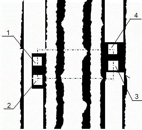
[0024] First, after the etching of the wafer and before the planarization of the copper connection holes, an electron beam defect scanner is used to establish a scanning program with appropriate conditions to scan the normal contrast copper connection holes and the under-etched copper connection holes of the wafer.

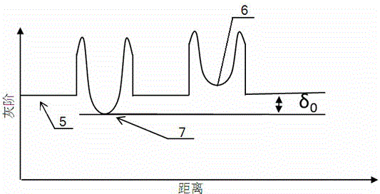
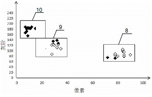
[0025] Next includes step 1 and step 2, such as image 3 As shown in , scan the pixel size and gray scale of the comparative copper connection hole, connection hole edge and background of the wafer, and determine the background area 8, the contrast copper connection hole area 9 and the connection hole edge area 10 from large to small pixels; And establish a two-dimensional distribution map ...


PUM


Abstract

The invention provides a method for improving a capture rate of under-etching defects. The method includes scanning a comparison copper connecting hole of a wafer, a connecting hole edge and the pixel size and a gray scale of a background, and determining a background region, a comparison copper connecting hole region and a connecting hole edge region; scanning a gray scale of an under-etching copper connecting hole of the wafer; and comparing the difference between the gray scale of the comparison copper connecting hole region and the gray scale of the under-etching copper connecting hole. According to the method, the capture rate of under-etching defects can be improved effectively in the production process so as to provide a basis for monitoring of the etching process, when batch experiments are needed to optimize the process, the technical support is provided for improvement measures, and guarantee is provided for shorting of the research and development cycle of products.

Description

technical field [0001] The invention relates to a method for scanning defects, in particular to a method for improving the capture rate of insufficiently etched defects through an electron beam defect scanner using a gray scale masking method. Background technique [0002] Insufficient etching of copper connection holes in semiconductors is an important killer defect in the back-end process. With the development of integrated circuit technology and the proportional reduction of key dimensions and the improvement of aspect ratio, for example, when the device is below 55nm, this kind of Defects are more and more likely to occur. [0003] However, most of the detection of this kind of defect is carried out after the copper is planarized. There are two shortcomings in this layer of detection: one is that the copper cannot be exposed to the air for a long time, and the other is that after the copper is filled and flattened, only 3 / 2 copper connection holes for detection, such a...

Claims


Application Information

Patent Timeline
Patent Type & Authority Patents(China)
IPC IPC(8): H01L21/66
Inventor 范荣伟刘永波倪棋梁龙吟陈宏璘
Owner SHANGHAI HUALI MICROELECTRONICS CORP
Why Eureka
Try Eureka