Diode silicon stack cutting process and special tool thereof

A cutting process and diode technology, applied in the direction of fine working devices, working accessories, manufacturing tools, etc., can solve the problems of processing efficiency, easy to fall flat, and unable to cut smoothly, so as to shorten the cutting cycle, improve product quality, The effect of improving work efficiency

Active Publication Date: 2013-02-27
江苏皋鑫电子有限公司
View PDF7 Cites 7 Cited by
  • Summary
  • Abstract
  • Description
  • Claims
  • Application Information

AI Technical Summary

Problems solved by technology

There are certain disadvantages in this process method: it cannot ensure that the silicon wafer is rotated accurately by 90 degrees, and the end face of the silicon grain after cutting is not perpendicular to the side surface, which affects subsequent processing and product quality; when using this method to make dies fo

Method used


Image

  • Diode silicon stack cutting process and special tool thereof
  • Diode silicon stack cutting process and special tool thereof
  • Diode silicon stack cutting process and special tool thereof

Examples


Embodiment Construction

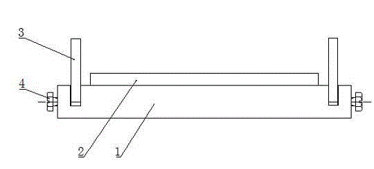
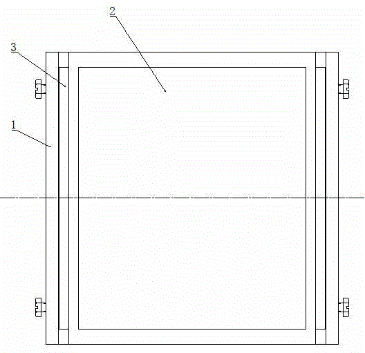
[0017] In the present invention, the silicon stacking tool is a conventional process fixture for the production of silicon grains in diode manufacturing enterprises, such as figure 1 , 2 As shown, it includes an aluminum mold base 1 , a glass bottom plate 2 , a glass baffle 3 and locking bolts 4 .

[0018] The aluminum mold base 1 is rectangular, and a glass bottom plate 2 is placed on its upper surface. The aluminum mold base 1 and the glass bottom plate 2 are connected by paraffin. There are through grooves on both sides of the aluminum mold base 1, and the lower end of the glass baffle 3 is embedded in the through groove. and locked and fixed by the locking bolt 4 on the side wall.

[0019] When cutting the diode silicon stack, the specific process is as follows:

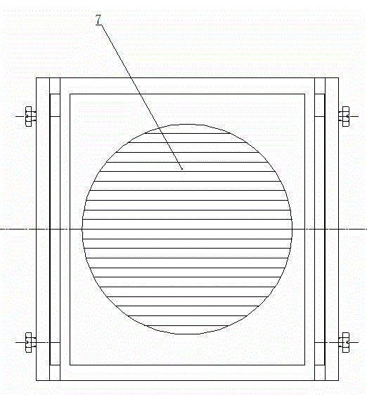
[0020] First, two layers of silicon stacks 7 are horizontally placed on the glass bottom plate 2 of the silicon stack bonding tool, and are fixed to the glass bottom plate 2 by paraffin to achieve one-time bond...


PUM


Abstract

The invention relates to a diode silicon stack cutting process and a special tool thereof. The process comprises steps of horizontally placing silicon stacks on a glass base plate of a silicon stack attaching tool, attaching the silicon stacks to the glass base plate through paraffin one time, placing the silicon stack attaching tool on a silicon chip cutter, conducting cutting to form a plurality of rows of silicon chips along the direction vertical to glass stopping plates on two sides of the silicon stack attaching tool by using the silicon chip cutter after the positioning, heating and melting the paraffin fixing silicon chips, rotating the silicon chips on the silicon stack attaching tool by 90 degrees in the plane direction, secondarily fixing silicon chips to the silicon stack attaching tool through the paraffin, placing the silicon stack attaching tool on the silicon chip cutter for secondary cutting, and cutting silicon chips to silicon particles. The process is simplified, silicon chips cannot be poured, the cutting period is shortened, the working efficiency is improved, silicon chips and silicon stacks can rotate by 90 degrees in the secondary attaching relative to the first attaching, and the product quality is improved.

Description

technical field [0001] The invention relates to a highly efficient and accurate diode silicon stack cutting process, and also relates to a special tool for realizing the diode silicon stack cutting process. Background technique [0002] There are many types of diodes, which can be divided into germanium diodes (Ge tubes) and silicon diodes (Si tubes) according to the semiconductor materials used. Silicon diodes have low reverse current, high temperature resistance, and are widely used. [0003] In the process of producing silicon diodes, the silicon stack needs to be cut into silicon grains. The process flow is as follows: firstly, the silicon stack is placed horizontally on the silicon stacking tool, and then the silicon stack and the silicon stacking tool are bonded by paraffin wax. Fix it to achieve one-time splicing; then install the silicon stack bonding device on the silicon wafer cutting machine, perform one cut, and cut the silicon stack into several rows of silico...

Claims


Application Information

Patent Timeline
IPC IPC(8): B28D5/04B28D7/04
Inventor 邱德强陈许平
Owner 江苏皋鑫电子有限公司
Why Eureka
Try Eureka