Liquid crystal display panel

A technology for liquid crystal display panels and substrates, which is applied in nonlinear optics, instruments, optics, etc., and can solve problems such as tipping and dark lines in spacers

Inactive Publication Date: 2020-06-19
SHENZHEN CHINA STAR OPTOELECTRONICS SEMICON DISPLAY TECH CO LTD
View PDF6 Cites 3 Cited by
  • Summary
  • Abstract
  • Description
  • Claims
  • Application Information

AI Technical Summary

Problems solved by technology

[0005] The embodiment of the present application provides a liquid crystal display panel to solve the problem that in the existing liquid crystal display panel, the liquid crystal in the space between the main pixel electrode and the sub-pixel electrode will be dumped at a large angle under the action of an electric field, resulting in Technical issue with dark lines at the spacer

Method used


Image

  • Liquid crystal display panel
  • Liquid crystal display panel
  • Liquid crystal display panel

Examples


Embodiment Construction

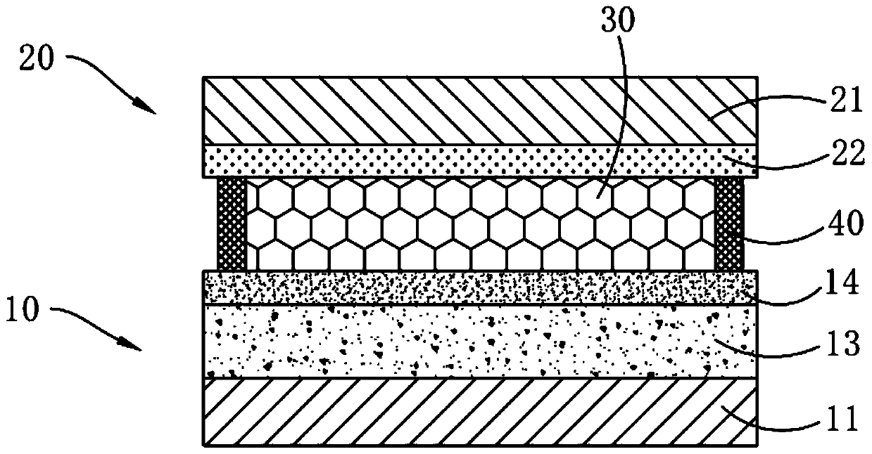
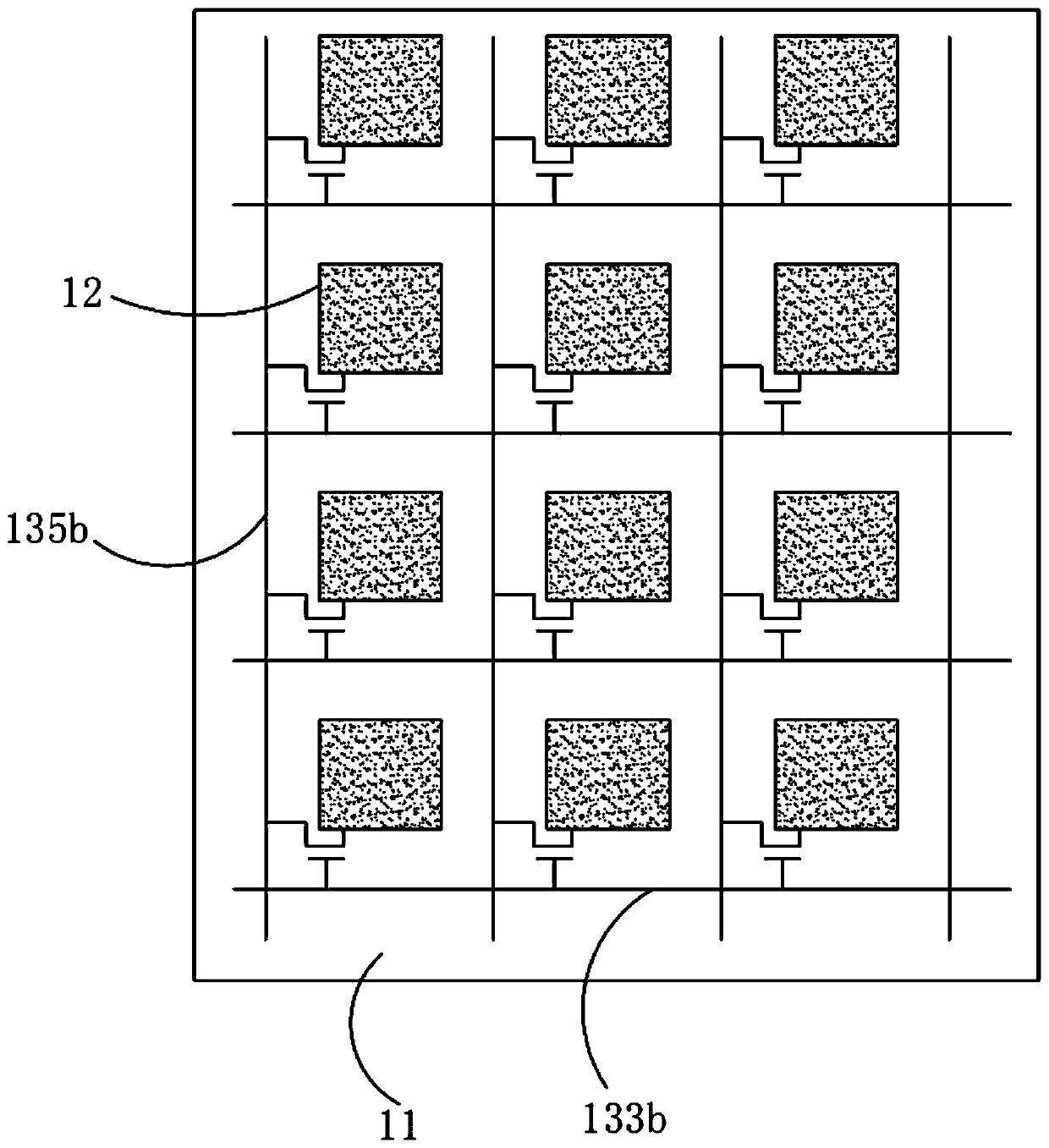
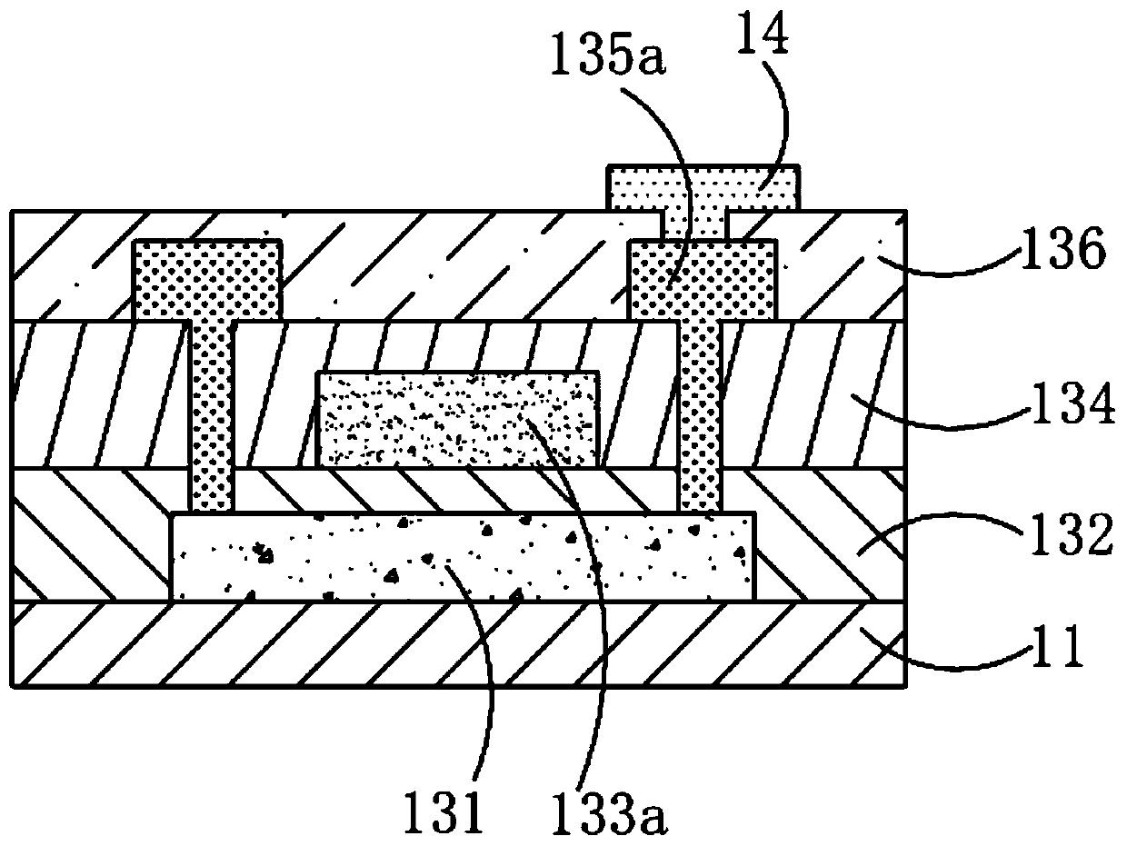
[0038] The technical solutions in the embodiments of the present application will be clearly and completely described below in conjunction with the drawings in the embodiments of the present application. Apparently, the described embodiments are only some of the embodiments of this application, not all of them. Based on the embodiments in this application, all other embodiments obtained by those skilled in the art without making creative efforts belong to the scope of protection of this application.

[0039] In the description of the present application, it should be understood that the terms "center", "longitudinal", "transverse", "length", "width", "thickness", "upper", "lower", "front", " Orientation indicated by rear, left, right, vertical, horizontal, top, bottom, inside, outside, clockwise, counterclockwise, etc. The positional relationship is based on the orientation or positional relationship shown in the drawings, which is only for the convenience of describing the a...


PUM

PropertyMeasurementUnit
lengthaaaaaaaaaa

Abstract

The invention discloses a liquid crystal display panel. The display panel comprises an array substrate and a color film substrate, and each pixel unit on the array substrate comprises a thin film transistor layer and a pixel electrode located on the thin film transistor layer. The pixel electrodes comprise a first pixel electrode and a second pixel electrode, and a spacer region is arranged between the first pixel electrode and the second pixel electrode, therefore, the influence of an electric field between the edge area of the first pixel electrode and the common electrode and an electric field between the edge area of the second pixel electrode and the common electrode on the liquid crystal at the interval area is reduced, and dark fringes generated at the interval area due to large-angle toppling of the liquid crystal at the interval area under the action of the electric fields are prevented.

Description

technical field [0001] The present application relates to the field of display technology, in particular to a liquid crystal display panel. Background technique [0002] MVA (Multi Vertical Alignment) liquid crystal display panel has been widely used due to its advantages of high contrast and wide viewing angle. A liquid crystal display panel generally includes an array substrate and a color filter substrate oppositely arranged, and a liquid crystal layer is arranged between the array substrate and the color filter substrate; pixel electrodes are arranged on the array substrate, and a common electrode is arranged on the color filter substrate. The electric field between them drives the liquid crystal to rotate. Each pixel unit on the array substrate generally includes a light-transmitting area and a non-light-transmitting area, the light-transmitting area is used for setting pixel electrodes, and the non-light-transmitting area is an arrangement area for connecting wires an...

Claims


Application Information

Patent Timeline
Patent Type & Authority Applications(China)
IPC IPC(8): G02F1/1343G02F1/1362G02F1/1368
CPCG02F1/134309G02F1/136204G02F1/136286G02F1/1368G02F2202/22G02F1/136218G02F1/134345G02F1/136222
Inventor 张琪曹武
Owner SHENZHEN CHINA STAR OPTOELECTRONICS SEMICON DISPLAY TECH CO LTD
Why Eureka
Try Eureka