Shift register and array substrate grid driving device

A shift register, gate connection technology, applied in static memory, digital memory information, instruments, etc., can solve problems such as poor stability, the OUTPUT terminal of the output terminal cannot work stably for a long time, and the noise at the output terminal cannot be completely solved.

Active Publication Date: 2013-02-27
HEFEI BOE OPTOELECTRONICS TECH +1
View PDF4 Cites 30 Cited by
  • Summary
  • Abstract
  • Description
  • Claims
  • Application Information

AI Technical Summary

Problems solved by technology

[0003] attached figure 1 It is the most basic unit of GOA, which is composed of 4 thin film transistors and 1 capacitor. In practical applications, the T2 transistor of this GOA unit will cause noise at the output terminal OUTPUT due to the influence of the coupling voltage generated by the first clock signal CLK on it. and cannot work stably for a long time
At present, many GOA patents have given some solutions to the above problems and can basically solve the above problems, but there is no GOA solution that can completely solve the noise and poor stability of the output.

Method used


Image

  • Shift register and array substrate grid driving device
  • Shift register and array substrate grid driving device
  • Shift register and array substrate grid driving device

Examples


Embodiment 1

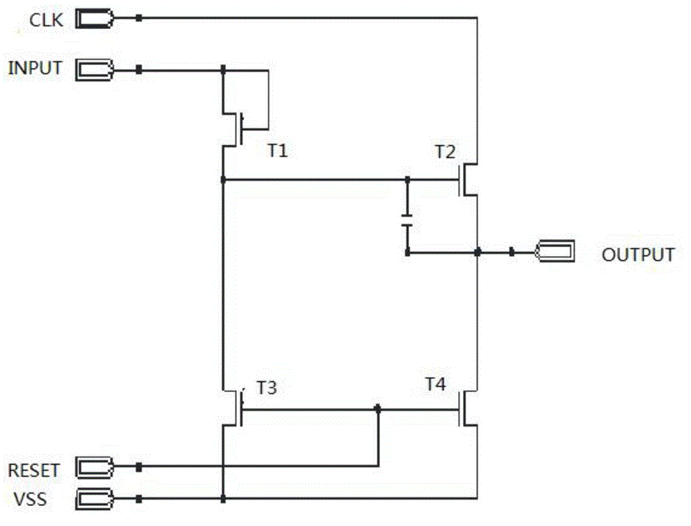
[0056] See attached figure 2 , Embodiment 2 of the present invention provides a shift register, including:

[0057] The input module 101, in response to the input signal INPUT, is used to provide the input signal voltage INPUT to the pull-up node PU point, wherein the pull-up node is the output node of the input module; including:

[0058] The source and gate of the first thin film transistor M1 are connected to the input signal terminal, and the drain is used as the output node of the input module, that is, as the pull-up node PU point;

[0059] The pull-up module 102 is used for storing the input signal voltage INPUT and providing the first clock signal voltage CLK to the output terminal OUTPUT in response to the pull-up node PU point; including:

[0060] The drain of the second thin film transistor M2 is connected to the first clock signal terminal CLK, the gate is connected to the pull-up node PU, and the source is connected to the output terminal OUTPUT;

[0061] Capac...

Embodiment 2

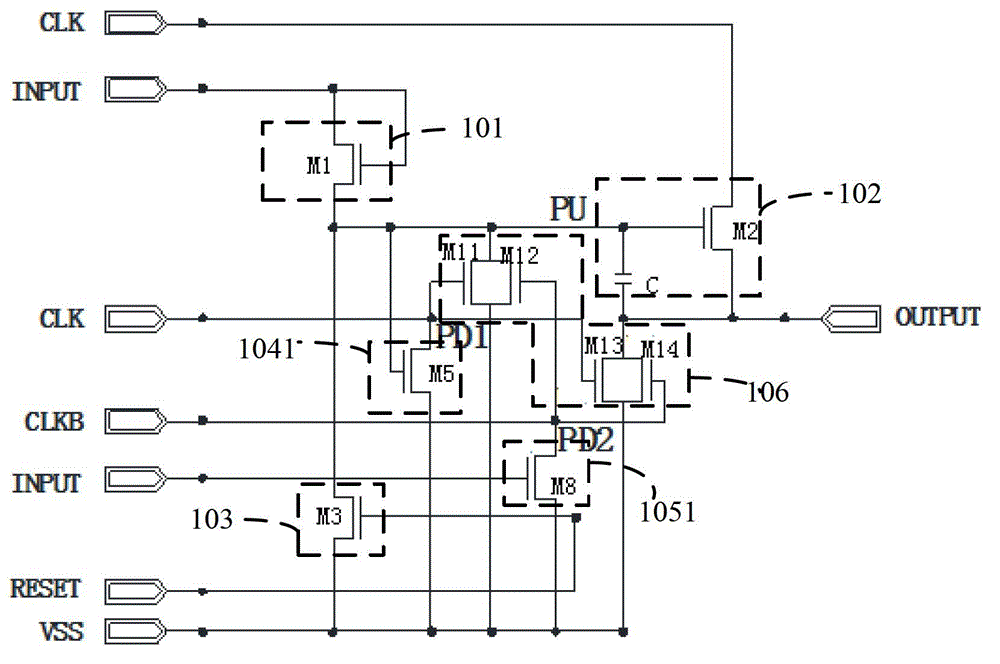
[0082] see Figure 4 , a shift register provided by Embodiment 2 of the present invention, comprising:

[0083] The input module 101, in response to the input signal INPUT, is used to provide the input signal voltage INPUT to the pull-up node PU point, wherein the pull-up node is the output node of the input module; including:

[0084] The source and gate of the first thin film transistor M1 are connected to the input signal terminal, and the drain is used as the output node of the input module, that is, as the pull-up node PU point;

[0085] The pull-up module 102 is used for storing the input signal voltage INPUT and providing the first clock signal voltage CLK to the output terminal OUTPUT in response to the pull-up node PU point; including:

[0086] The drain of the second thin film transistor M2 is connected to the first clock signal terminal CLK, the gate is connected to the pull-up node PU, and the source is connected to the output terminal OUTPUT;

[0087] Capacitor ...


PUM


Abstract

The invention discloses a shift register and a grid driving device, which are used for eliminating noise of an output terminal of the shift register and improving the working stability of the shift register. The shift register provided by the invention comprises an input module, a pull-up module, a reset module, a first pull-down control module, a second pull-down control module and a pull-down module, wherein the input module is used for supplying input signal voltage to a pull-up node, which is an output node of the input module; the pull-up module is used for storing the input signal voltage and supplying first clock signal to an output terminal; the reset module is used for supplying power source cathode voltage to the pull-up node; the first pull-down control module is used for supplying the power source cathode voltage to a first pull-down node; the second pull-down control module is used for supplying the power source cathode voltage to a second pull-down node; and the pull-down module is used for supplying the power source cathode voltage to the pull-up node and the output terminal.

Description

technical field [0001] The invention relates to the technical field of liquid crystal display driving, in particular to a shift register, a driving method thereof, and a gate driving device. Background technique [0002] Flat-panel displays have been vigorously promoted because of their ultra-thin energy saving. Shift registers are used in most flat-panel displays. By integrating the gate drive device into the liquid crystal panel (gate on array, GOA) method, the shift register can save the gate drive IC and reduce a manufacturing process. , so not only the production cost of the flat panel display is reduced, but also the production cycle is shortened to a certain extent. Therefore, GOA technology has been widely used in flat panel display manufacturing in recent years. The service life of GOA and its output stability have always been a concern in the design of GOA. [0003] attached figure 1 It is the most basic unit of GOA, which is composed of 4 thin film transistors...

Claims


Application Information

Patent Timeline
Patent Type & Authority Applications(China)
IPC IPC(8): G09G3/20G09G3/36G11C19/28
CPCG11C19/28
Inventor 杨通马睿胡明
Owner HEFEI BOE OPTOELECTRONICS TECH
Why Eureka
Try Eureka