Array substrate, display panel as well as display device and driving method thereof

An array substrate and driving end technology, which is applied in the fields of array substrates, display devices and their drivers, and display panels, can solve problems such as the inability to balance cost and display effect, and achieve the effect of improving quality

Active Publication Date: 2013-03-06
BOE TECH GRP CO LTD +1
View PDF11 Cites 8 Cited by
  • Summary
  • Abstract
  • Description
  • Claims
  • Application Information

AI Technical Summary

Problems solved by technology

[0008] The object of the present invention is to provide an array substrate, a display panel, a display device and a driving method thereof, so as to solve the problem that the cost of the inversion driving circuit and the display effect of the Dual Gate structure display device in the prior art cannot be balanced

Method used


Image

  • Array substrate, display panel as well as display device and driving method thereof
  • Array substrate, display panel as well as display device and driving method thereof
  • Array substrate, display panel as well as display device and driving method thereof

Examples


Embodiment Construction

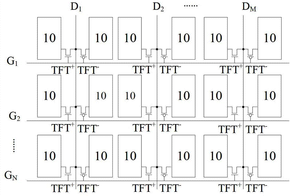
[0028] In order to use the column inversion driving method to realize the display effect of dot inversion and achieve low cost and high display picture quality, on the basis of the traditional array substrate with Dual Gate structure, the embodiment of the present invention provides a new array substrate structure, including : gate lines, data lines, pixel electrodes and pixel switches.

[0029] by figure 2 The array substrate shown as an example, including the gate lines (G 1 , G 2 , G 3 ), data line (D 1 、D 2 、D 3 ), pixel electrode (P 11 ~P 36 ) and pixel switches (201 and 202), the source of each pixel switch is connected to a pixel electrode, and the two columns of pixel electrodes located on both sides of the same data line and adjacent to the data line are connected to each other through the drain of the pixel switch The data lines are connected, and each row of pixel electrodes is connected to a gate line through the gate of the pixel switch.

[0030] In the ...


PUM


Abstract

The invention relates to the technical field of display, and discloses an array substrate, a display panel as well as a display device and a driving method thereof. The array substrate comprises a grid line, a data line, pixel electrodes and pixel switches; a source electrode of each pixel switch is connected with one pixel electrode; two columns of pixel electrodes which are located on the both sides of the same data line and are adjacent to the data line are connected with the data line through the drain electrodes of the pixel switches; each row of pixel electrode is connected with the grid line through the grid electrodes of the pixel switches; as for two adjacent pixel electrodes in the same row, one is connected with the pixel switch started by grid positive voltage, and the other one is connected with the pixel switch started by grid negative voltage; and as for two adjacent pixel electrodes in the same column, one is connected with the pixel switch started by the grid positive voltage, and the other one is connected with the pixel switch started by the grid negative voltage. According to the invention, a column inversion driving circuit with low cost is used, so that a point inversion display effect can be realized, and the quality of a display picture can be improved.

Description

technical field [0001] The present invention relates to the field of display technology, in particular to an array substrate, a display panel, a display device and a driving method thereof. Background technique [0002] Array substrates of TFT-LCD (Thin Film Field Effect Transistor-Liquid Crystal Display), OLED (Organic Light Emitting Diode) display devices, electronic paper and other display devices adopt row-column matrix driving mode, which is specifically formed by crossing N rows of gate lines and M columns of data lines A matrix of rows and columns, and TFTs (Thin Film Field Effect Transistors) are arranged at each intersection, and the control of each pixel electrode in the matrix of rows and columns is realized through TFTs. [0003] On the premise that the resolution remains unchanged, in order to reduce the cost of the product, it may be considered to reduce the number of data lines. To achieve this goal, the prior art proposes a method such as figure 1 The speci...

Claims


Application Information

Patent Timeline
IPC IPC(8): G02F1/1362G02F1/1368G02F1/1333G09G3/36
Inventor王本莲祁小敬蒋冬华
OwnerBOE TECH GRP CO LTD