
Eureka
For R&D, Eureka makes reading and utilizing patents & technical documents easy.
Eureka AIR
Designed for self-driven R&D workflows. Generate viable solutions, solve complex R&D challenges, empower your innovation with AI.

Eureka Materials
Designed for material experts only. Revolutionize your material R&D, from search, analyze, to developing new materials.

TechResearch
Generate reliable direction feasibility study reports for your R&D in just a few steps.

TechSeek
Discover and master advanced knowledge NOW. Basics, ideas, possibilities, all at once.

TechMind
As an expert in R&D Theories, TechMind can generates customized viable solutions instantly.

TechRisk
Analyze your overall solution with one click, know your potential R&D risks in advance.

TechMonitor
Get weekly tech updates, stay abreast of the latest tech innovations and key insights.
Lithographic apparatus, substrate table and device manufacturing method
A substrate table and substrate technology, applied in the field of manufacturing devices, can solve problems such as deformation, calculation errors, hindrances to miniaturization and the use of multiple detectors
- Summary
- Abstract
- Description
- Claims
- Application Information
AI Technical Summary
Problems solved by technology
Method used
Image

Examples
Embodiment Construction
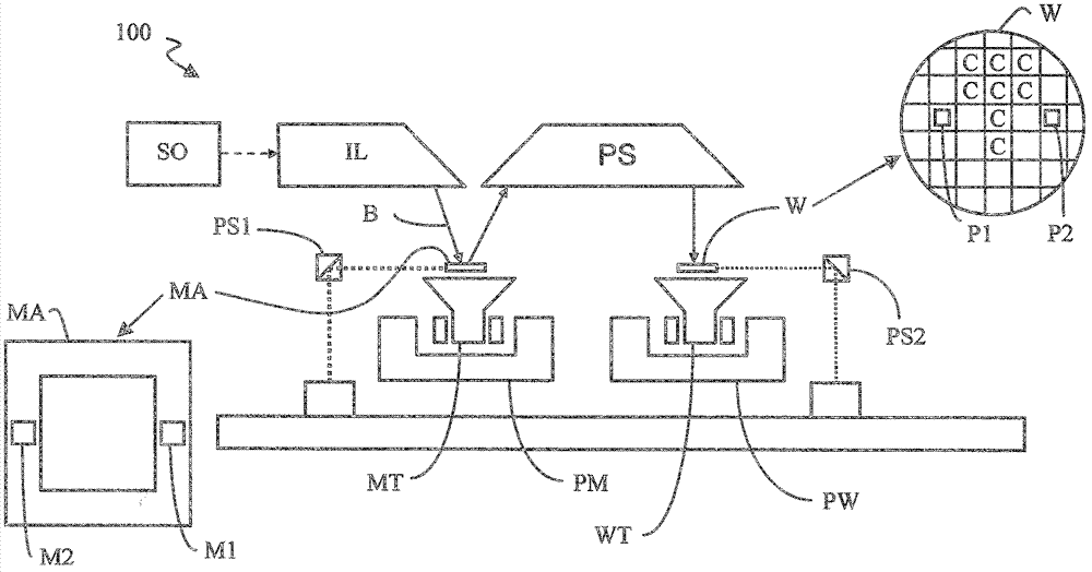
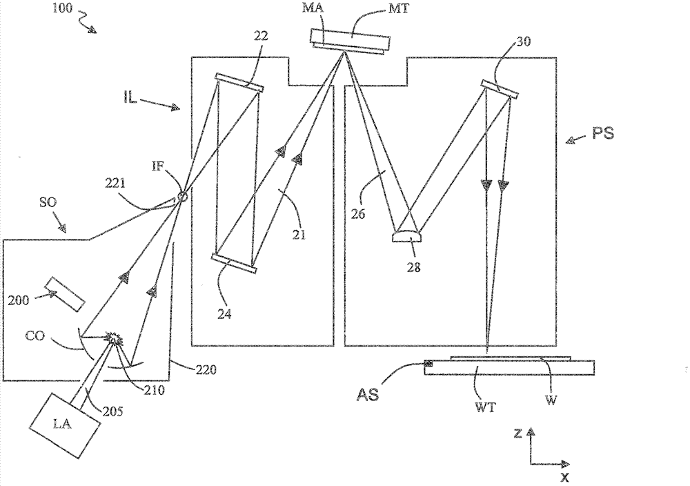
[0044] figure 1 A lithographic apparatus 100 comprising a source collector module SO according to an embodiment of the present invention is schematically shown. The lithographic apparatus comprises: an illumination system (illuminator) IL configured to condition a radiation beam B (e.g. EUV radiation); a support structure (e.g. a mask table) MT configured to support a patterning device (e.g. A mask or reticle) MA, and is connected to a first positioning device PM configured to accurately position the patterning device MA; a substrate table (such as a wafer stage) WT, which is configured to hold a substrate (such as coated with Resist wafer) W, and is connected with the second positioning device PW that is configured to accurately position substrate W; The pattern of beam B is projected onto a target portion C of substrate W (eg, comprising one or more dies).
[0045] The illumination system may include various types of optical components, such as refractive, reflective, magn...
PUM
| Property | Measurement | Unit |
|---|---|---|
| thickness | aaaaa | aaaaa |
| thickness | aaaaa | aaaaa |
Abstract
Description
Claims
Application Information
 - R&D Engineer
- R&D Manager
- IP Professional
- Industry Leading Data Capabilities
- Powerful AI technology
- Patent DNA Extraction
Browse by: Latest US Patents, China's latest patents, Technical Efficacy Thesaurus, Application Domain, Technology Topic, Popular Technical Reports.
© 2024 PatSnap. All rights reserved.Legal|Privacy policy|Modern Slavery Act Transparency Statement|Sitemap|About US| Contact US: help@patsnap.com