Forming method of grid electrode

A grid and gate electrode technology, which is applied in the photoplate making process of the pattern surface, microlithography exposure equipment, optics, etc., can solve the problem of shortening of the line end, and achieve the effect of improving the yield rate and improving the shortening of the line end

Active Publication Date: 2015-03-11
SEMICON MFG INT (SHANGHAI) CORP
View PDF7 Cites 0 Cited by
  • Summary
  • Abstract
  • Description
  • Claims
  • Application Information

AI Technical Summary

Problems solved by technology

[0011] For more information about LELE technology, please refer to the US patent No. US6042998, but this patent does not address the problem of shortening the line ends when etching to form the gate.

Method used


Image

  • Forming method of grid electrode
  • Forming method of grid electrode
  • Forming method of grid electrode

Examples


Embodiment Construction

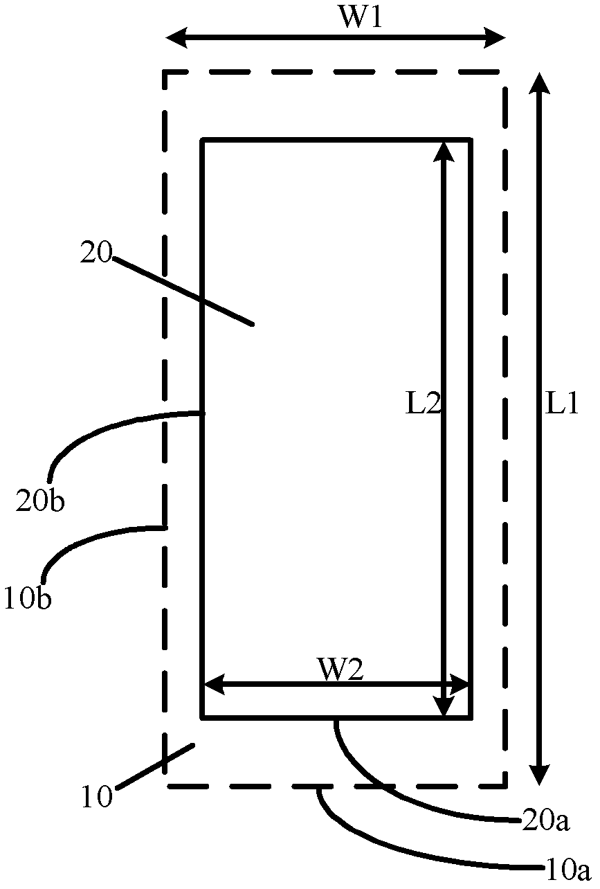
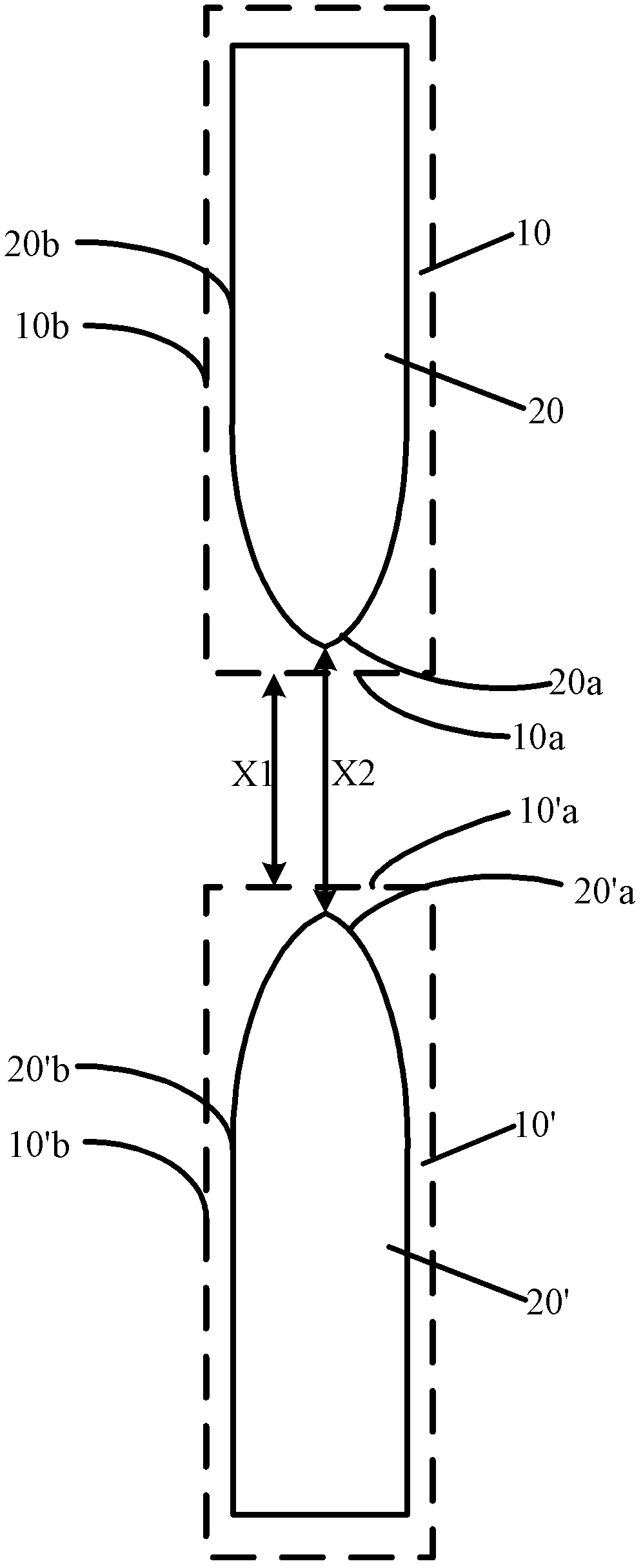
[0036] As mentioned in the background art, in the etching process of the prior art to form the gate, there will be a more obvious problem of shortening of the line ends. As the feature size (CD, Critical Dimension) of semiconductor devices becomes smaller and smaller, double patterning Forming the gate by the method can prevent the end of the line and the side end of the line from being etched at the same time, but the problem of shortening the end of the line has not been effectively solved.

[0037] In order to improve the problem of shortening of the line ends in the process of forming the gate by etching, the present invention provides a method for forming the gate.

[0038] In order to make the above objects, features and advantages of the present invention more comprehensible, specific implementations of the present invention will be described in detail below in conjunction with the accompanying drawings.

[0039] In the following description, specific details are set fo...


PUM


Abstract

The invention provides a forming method of a grid electrode, which comprises the steps of: providing a substrate, wherein a grid dielectric layer, a grid electrode layer, an intermediate layer, a polycrystalline silicon layer and a first pattern layer comprising a first pattern are sequentially formed on the surface of the substrate, and the distance between line ends of the grid electrode to be formed is defined by the first pattern; doping ions into the polycrystalline silicon layer by using the first pattern layer as a mask; eliminating the first pattern layer and the polycrystalline silicon layer with the doped ions, and forming an opening; forming a second pattern layer covering the opening and the surface of the polycrystalline silicon layer, wherein the second pattern layer is provided with a second pattern, and the line width of the grid electrode to be formed is defined by using the second pattern; etching the polycrystalline silicon layer by using the second pattern layer with the second pattern as a mask, and forming a polycrystalline silicon layer comprising a third pattern; and etching the intermediate layer and the grid electrode layer by using the polycrystalline silicon layer with the third pattern as a mask to form the grid electrode. According to the embodiment of the invention, the problem of line end reduction in the grid electrode process is solved, and the yield is increased.

Description

technical field [0001] The invention relates to the field of semiconductor manufacturing, in particular to a method for forming a gate. Background technique [0002] With the continuous development of semiconductor manufacturing technology, the feature size (CD, Critical Dimension) of semiconductor devices in integrated circuits is getting smaller and smaller, and transistors and metal lines are getting smaller and closer together. The line end shortening (LES, Line End Shortening) is a more important problem, and LES is expressed as the difference between the actual printing position and the predetermined (design) position of the line end. [0003] figure 1 shows the problem of line-end shortening, as figure 1 As shown, the dotted line shows the expected (design) formed circuit 10, but due to the etching effect and photoresist pullback (Photo Resist Pullback) and other reasons, a significant number of actual circuits 20 with shortened line ends are produced. The expected...

Claims


Application Information

Patent Timeline
Patent Type & Authority Patents(China)
IPC IPC(8): H01L21/28G03F7/00G03F7/20
Inventor 张海洋顾一鸣
Owner SEMICON MFG INT (SHANGHAI) CORP
Why Eureka
Try Eureka