Method for forming gate electrode

A gate and gate layer technology, applied in semiconductor devices and other directions, can solve problems such as shortening of wire ends, and achieve the effect of improving yield and shortening wire ends

Active Publication Date: 2012-08-29
SEMICON MFG INT (SHANGHAI) CORP
View PDF11 Cites 30 Cited by
  • Summary
  • Abstract
  • Description
  • Claims
  • Application Information

AI Technical Summary

Problems solved by technology

[0011] The problem to be solved by the present invention is the problem of shortening of the line ends during the process of etching and forming the gate in the prior art

Method used


Image

  • Method for forming gate electrode
  • Method for forming gate electrode
  • Method for forming gate electrode

Examples


Embodiment Construction

[0035] In order to make the above objects, features and advantages of the present invention more comprehensible, specific implementations of the present invention will be described in detail below in conjunction with the accompanying drawings.

[0036] In the following description, specific details are set forth in order to provide a thorough understanding of the present invention. However, the present invention can be implemented in many other ways than those described here, and those skilled in the art can make similar extensions without departing from the connotation of the present invention. Accordingly, the present invention is not limited to the specific embodiments disclosed below.

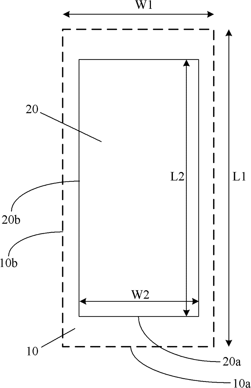
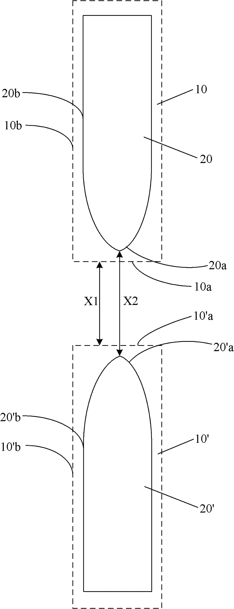
[0037]In the gate formation process of etching in the prior art, there will be a more obvious problem of line terminal shortening. As the feature size (CD, Critical Dimension) of semiconductor devices becomes smaller and smaller, even if the gate is formed by double patterning, Although it...


PUM


Abstract

The invention relates to a method for forming a gate electrode. The method comprises the following steps of: sequentially forming a gate dielectric layer, a gate electrode layer and a barrier layer on a substrate; forming a first mask layer for covering the barrier layer and impressing to form the first mask layer with a first pattern comprising at least one opening which defines a distance between tail ends of a line which is to form the gate electrode; depositing an antireflective layer filling the opening in and covering the first mask layer; forming a second mask layer for covering the antireflective layer, and patterning to form the second mask layer with a second pattern which defines a line width which is to form the gate electrode; taking the second mask layer with the second pattern as a mask to etch the antireflective layer and the first mask layer to for a first mask layer with a third patter; and taking the first mask layer with the third pattern as a mask to etch the barrier layer and the gate electrode layer to form the gate electrode. Through the method provided by the invention, the line-end shortening problem in the gate electrode etching forming process can be improved, and the yield can be improved.

Description

technical field [0001] The invention relates to the field of semiconductor manufacturing, in particular to a method for forming a gate. Background technique [0002] With the continuous development of semiconductor manufacturing technology, the feature size (CD, Critical Dimension) of semiconductor devices in integrated circuits is getting smaller and smaller, and transistors and metal lines are getting smaller and closer together. The line end shortening (LES, Line End Shortening) is a more important problem, and LES is expressed as the difference between the actual printing position and the predetermined (design) position of the line end. figure 1 shows the problem of line-end shortening, as figure 1 As shown, the dotted line shows the predetermined (designed) formation of the expected line 10, but due to etching effects and photoresist pullback (PhotoResist Pullback) and other reasons, a significant number of actual lines 20 with shortened line ends are produced. The ex...

Claims


Application Information

Patent Timeline
Patent Type & Authority Applications(China)
IPC IPC(8): H01L21/28
Inventor 张海洋符雅丽王新鹏
Owner SEMICON MFG INT (SHANGHAI) CORP
Why Eureka
Try Eureka