Array substrate, and 3D display device and drive method thereof

A technology of an array substrate and a driving method, which is applied in the field of 3D display, can solve problems such as rising product cost, lowering display device transmittance, and low yield rate of display device products, so as to reduce charging time, ensure charging time, and improve refresh rate. The effect of frequency

Inactive Publication Date: 2013-03-20
BOE TECH GRP CO LTD +1
View PDF4 Cites 3 Cited by
  • Summary
  • Abstract
  • Description
  • Claims
  • Application Information

AI Technical Summary

Problems solved by technology

In order to ensure the charging rate of the pixel electrode, it is often necessary to increase the line width of the wire on the display device to reduce the load on the display device, which will reduce the transmittance of the display device; and the product yield of the display device with a high refresh rate is not high. resulting in an increase in the cost of the product

Method used


Image

  • Array substrate, and 3D display device and drive method thereof
  • Array substrate, and 3D display device and drive method thereof

Examples


Embodiment 1

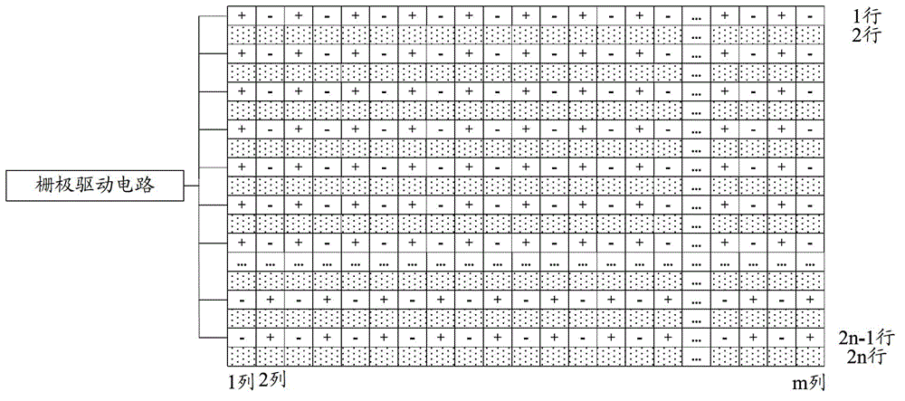
[0028] When the refresh frequency of the display device is 60Hz, assuming that there are 1126 rows of pixel units on the array substrate, the turn-on time of each row of pixel units is 1 / (1126*60)s, which is about 14.8us, in order to To realize 3D display, it is necessary to increase the refresh frequency of the display device to 120Hz, so that the charging time of the pixel electrodes will be reduced. In order to ensure the charging rate of the pixel electrodes, in the prior art, it is often necessary to increase the line width of the wires on the array substrate to reduce The load on the display device will reduce the transmittance of the display device; and the response time of the display device with a high refresh rate is insufficient, resulting in poor picture quality.

[0029] In order to avoid the above-mentioned problems, this embodiment provides an array substrate, including a substrate, and 2n rows of pixel units formed on the substrate in matrix form, and the array ...

Embodiment 2

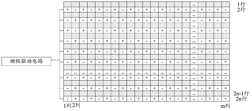
[0043] When the refresh frequency of the display device is 60Hz, assuming that there are 1126 rows of pixel units on the array substrate, the turn-on time of each row of pixel units is 1 / (1126*60)s, which is about 14.8us, in order to To realize 3D display, it is necessary to increase the refresh frequency of the display device to 120Hz, so that the charging time of the pixel electrodes will be reduced. In order to ensure the charging rate of the pixel electrodes, in the prior art, it is often necessary to increase the line width of the wires on the array substrate to reduce The load on the display device will reduce the transmittance of the display device; and the response time of the display device with a high refresh rate is insufficient, resulting in poor picture quality.

[0044] In order to avoid the above-mentioned problems, this embodiment provides an array substrate, including a substrate, and 2n rows of pixel units formed on the substrate in matrix form, and the array ...


PUM


Abstract

The invention provides an array substrate, and a 3D display device and a drive method thereof, belonging to the field of 3D display. The array substrate comprises a substrate, 2n lines of pixel units formed on the substrate by adopting a matrix mode, and also comprises gate lines corresponding to the 2n lines of pixel units, wherein each gate line is connected with a gate electrode of a thin film transistor in the corresponding pixel unit, the gate line corresponding to the (2k-1)th line of pixel units is used for receiving a gate electrode scanning signal according to a preset time period, or the gate line corresponding to the (2k)th line of pixel units is used for receiving the gate electrode scanning signal according to the preset time period, and k is a natural number of not less than 1 and not more than n. According to the technical scheme, the refreshing frequency of a display panel can be increased, the charging time of pixel electrodes is ensured, and the 3D display is realized.

Description

technical field [0001] The present invention relates to the field of 3D display, in particular to an array substrate, a 3D display device and a driving method thereof. Background technique [0002] With the development of display technology, 3D display technology has become one of the important technologies of display devices. Active shutter 3D display technology is a low-cost 3D display method. It achieves 3D effects by increasing the refresh rate of the screen, and cooperates with the rapid switching of 3D glasses so that the viewer's eyes can watch the corresponding left, right eye image to form a stereoscopic image effect. [0003] Due to the requirement of the human eye for receiving continuous images, it is necessary to provide each eye with an image of at least 60 Hz. Therefore, the refresh frequency of the display device must reach 120 Hz. Correspondingly, the driving frequency of the display device driving circuit also needs to be increased to 120 Hz. The charging...

Claims


Application Information

Patent Timeline
IPC IPC(8): G02F1/1362G02F1/133G09G3/36G02B27/22
CPCG09G3/003G09G2310/0254G09G2340/0435H04N13/144
Inventor 张亮邵喜斌王丹胡巍浩许益祯侯帅
Owner BOE TECH GRP CO LTD
Why Eureka
Try Eureka