Peeling device and manufacturing method for electronic device

A peeling device and manufacturing method technology, which are applied in the fields of semiconductor/solid-state device manufacturing, chemical instruments and methods, electrical components, etc., can solve problems such as cracking of reinforcing plates, and achieve the effect of suppressing damage

Inactive Publication Date: 2013-03-20
ASAHI GLASS CO LTD
View PDF3 Cites 18 Cited by
  • Summary
  • Abstract
  • Description
  • Claims
  • Application Information

AI Technical Summary

Problems solved by technology

Due to this load, at least one of the above-mentioned base plate and reinforcing plate may be cracked from the edge

Method used


Image

  • Peeling device and manufacturing method for electronic device
  • Peeling device and manufacturing method for electronic device
  • Peeling device and manufacturing method for electronic device

Examples


no. 1 Embodiment approach

[0050] In order to cope with the thinning of substrates used in electronic devices, the method of manufacturing an electronic device according to this embodiment includes a step of forming a functional layer on a substrate reinforced with a reinforcing plate, and separating the substrate on which the functional layer is formed and the reinforcing plate. The stripping process. Stiffeners do not form part of the electronics.

[0051] Here, the electronic device refers to electronic components such as a display panel, a solar cell, and a thin-film rechargeable battery. The display panel includes a liquid crystal panel (LCD), a plasma panel (PDP), and an organic EL panel (OLED).

[0052](Laminates)

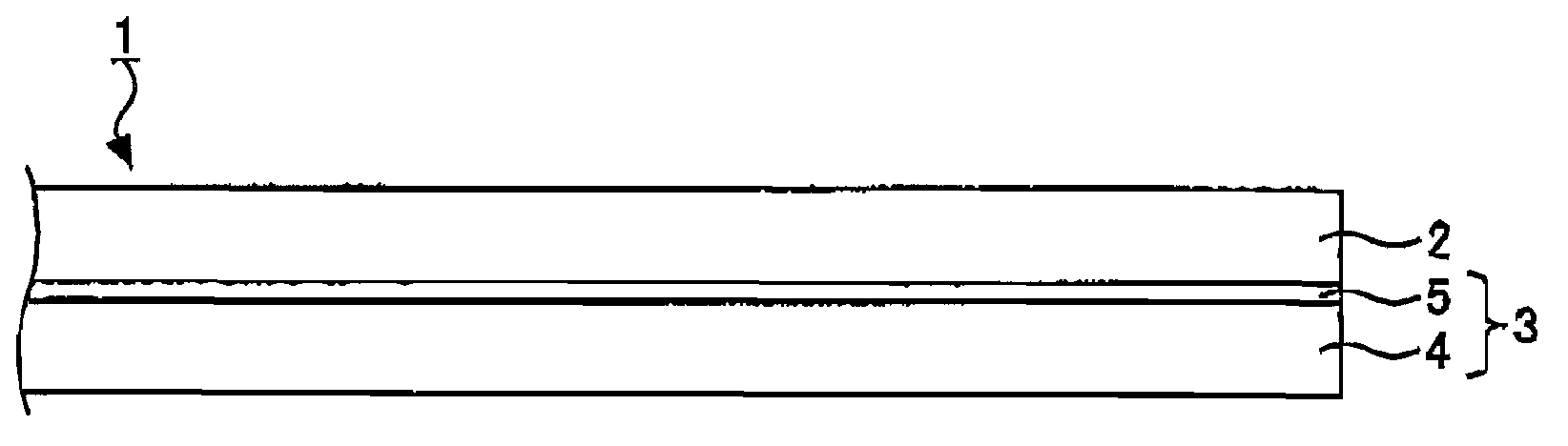
[0053] figure 1 It is a side view of a laminated board used in the manufacturing process of an electronic device. The laminated board 1 includes a base plate 2 and a reinforcement plate 3 for reinforcing the base plate 2 .

[0054] (substrate)

[0055] During the manufacturing p...

no. 2 Embodiment approach

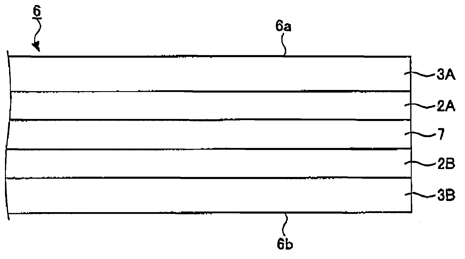
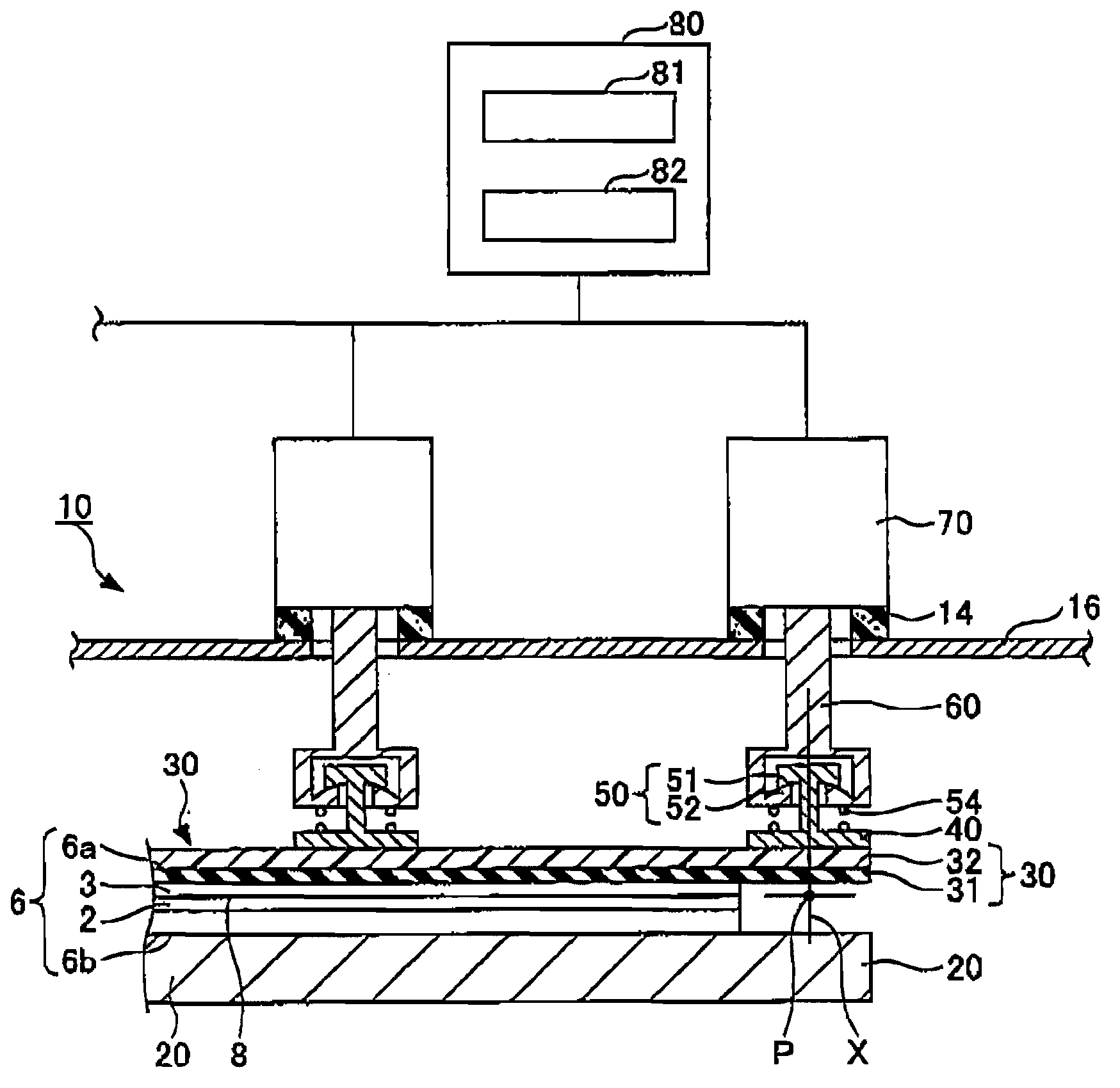
[0139] In the above-described first embodiment, the flexible plate 30 , the plurality of movable bodies 40 , the plurality of links 60 , the plurality of driving devices 70 , and the like are arranged on one side of the laminated body 6 .

[0140] On the other hand, in the present embodiment, flexible plates 30 , a plurality of movable bodies 40 , a plurality of links 60 , a plurality of driving devices 70 , and the like are arranged on both sides of the laminated body 6 .

[0141] Figure 8 It is a partial sectional view showing the peeling device of the second embodiment. Figure 9 yes means Figure 8 A partial cross-sectional view of an example of the operation of the peeling device. Figure 10 (a)~(f) means using Figure 8 An example of the peeling process of the peeling device.

[0142] The peeling apparatus 110 of this embodiment has the 1st flexible plate 30A arrange|positioned at one side of the laminated body 6, the some 1st movable body 40A, the some 1st link 60A...

no. 3 Embodiment approach

[0158] In this embodiment, although it is used in the same manner as in the second embodiment Figure 8 The peeling device shown performs the peeling, but the behavior of the peeling device is different.

[0159] Figure 11 (a)~(f) means using Figure 8 The figure of other peeling process of the peeling device.

[0160]The laminated body 6 is placed on the second flexible board 30B with the reinforcement board 3A on the upper side. The control device 80 lowers the first frame body 16A to a predetermined position, and presses the first flexible board 30A against the reinforcement board 3A. Next, the control device 80 vacuum-adsorbs the reinforcing plate 3A using the first flexible plate 30A. In this state, if Figure 11 (a) and Figure 8 As shown, the first and second flexible plates 30A, 30B are in flat plate shape.

[0161] Next, if Figure 11 As shown in (b) and (c), the control device 80 bends and deforms the first flexible plate 30A so as to peel off the interface ...


PUM


Abstract

The invention provides a peeling device and a manufacturing method for electronic devices. The peeling device peels a substrate and an interface of a reinforcing plate which reinforces the substrate from an end to the other end in sequence. The peeling device comprises a bearing component which supports the above substrate and a first main surface of a laminate of thereinforcing plate, a flexible plate which absorbs a second main surface of the laminate, a plurality of movable bodies which are fixed on the flexible plate at intervals and can independently move relative to the bearing component, and a control device which controls movement of the plurality of movable bodies. The control device controls movement of the plurality of movable bodies in a following method. When a straight-line distance between two ends of a border line of a part which is peeled off theinterface and a part which is not peeled off theinterface is longest, the above border line forms a bending shape raised to the rear of a moving direction of the border line.

Description

technical field [0001] The present invention relates to a peeling device for peeling a substrate and a reinforcing plate and a method for manufacturing an electronic device. Background technique [0002] As electronic devices such as display panels, solar cells, and thin-film rechargeable batteries become thinner and lighter, substrates used in electronic devices are required to be thinner. If the substrate becomes thinner, the handleability of the substrate deteriorates, so it is difficult to form functional layers for electronic devices (such as thin film transistors and color filters) on the substrate. [0003] Therefore, a method of peeling the substrate and the reinforcing plate after forming a functional layer on the substrate reinforced with the reinforcing plate has been developed (for example, refer to Patent Document 1). At least one of the base plate and the reinforcing plate is flexurally deformed so that the interface between the base plate and the reinforcing ...

Claims


Application Information

Patent Timeline
Patent Type & Authority Applications(China)
IPC IPC(8): H01L21/02H01L31/18
CPCY02P70/50B32B38/10B32B43/006
Inventor 滝内圭伊藤泰则宇津木洋
Owner ASAHI GLASS CO LTD
Why Eureka
Try Eureka