Array substrate and display device

An array substrate and substrate technology, which is applied in static indicators, instruments, electrical components, etc., can solve the problems of large space, affecting the effect of narrow frame, and large size of GOA circuit, so as to reduce the size of the frame, increase the effective display area, reduce the The effect of the small border area

Active Publication Date: 2013-03-20
BOE TECH GRP CO LTD +1
View PDF4 Cites 42 Cited by
  • Summary
  • Abstract
  • Description
  • Claims
  • Application Information

AI Technical Summary

Problems solved by technology

[0003] However, the size of the existing GOA circuit is large and takes up a large space. As a result, it is difficult to furthe

Method used


Image

  • Array substrate and display device
  • Array substrate and display device
  • Array substrate and display device

Examples


Example Embodiment

[0039] Example

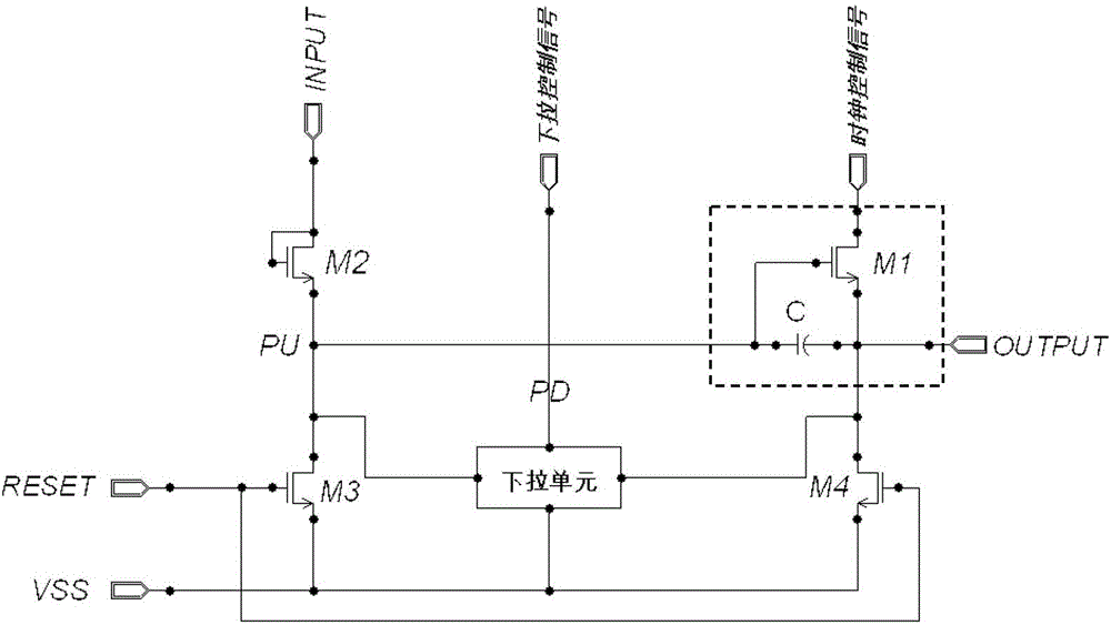
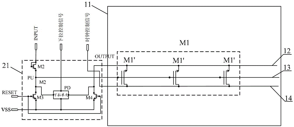
[0040] Such as figure 1 As shown, it is a shift register used in a gate drive circuit. A plurality of shift registers are cascaded to form a gate drive circuit. The embodiment of the present invention provides an array substrate with a narrow frame, such as figure 2 As shown, the array substrate includes: a substrate (not shown in the figure), a gate line 12 (only one row is shown in the figure) provided on the substrate, and a shift register that outputs a gate drive signal to the gate line 12 (Only one is shown in the figure); The shift register includes:

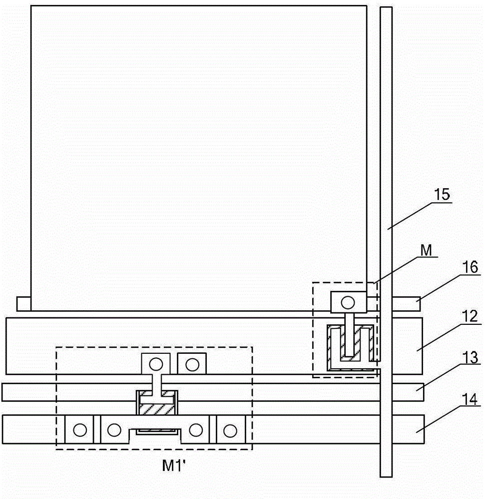
[0041] At least one first thin film transistor M1' is connected to the gate line 12;

[0042] The clock control signal line 14 and the first signal line 13 extend to the display area 11 of the array substrate;

[0043] The at least one first thin film transistor M1' is distributed in the display area 11 of the array substrate. The source of the first thin film transistor M1' is connected to the clock control sig...


PUM


Abstract

The invention discloses an array substrate and a display device with the array substrate and relates to the field of display, which can further reduce the peripheral frame size and realize the narrow frame so as to increase the effective display area of the display device. The array substrate comprises a substrate, a grid line and a shift register, wherein the grid line is arranged on the substrate; the shift register comprises at least one first thin film transistor, a time control signal line and a first signal line; the first thin film transistor is connected with the grid line; the time control signal line and the first signal line extend into a display area of the array substrate; at least one thin film transistor is distributed in the display area of the array substrate; a source electrode of the first thin film transistor is connected with the clock control signal line; a drain electrode of the first thin film transistor is connected with the grid line; and a grid electrode of the first thin film transistor is connected with the first signal line.

Description

technical field [0001] The present invention relates to the display field, in particular to an array substrate and a display device including the array substrate. Background technique [0002] The Gate Driver on Array (GOA) technology is a process technology that directly integrates gate driver ICs on the array substrate instead of an external driver chip. The application of this technology can not only reduce the production process, reduce product cost, improve integration, but also achieve a symmetrical and beautiful design on both sides of the panel, and also save the bonding (Bonding) area of ​​the gate circuit (Gate IC) and Fan-out (Fan-out) wiring space, so as to realize the design of narrow frame, improve production capacity and yield rate. [0003] However, the size of the existing GOA circuit is large and takes up a large space. As a result, it is difficult to further reduce the frame size of the existing LCD panel using the GOA integration technology, which affect...

Claims


Application Information

Patent Timeline
IPC IPC(8): H01L27/02G09G3/20
Inventor 王峥
Owner BOE TECH GRP CO LTD
Why Eureka
Try Eureka