Display device and array substrate and fabrication method of array substrate

An array substrate and peripheral wiring technology, which is applied in semiconductor/solid-state device manufacturing, optics, instruments, etc., can solve the problems that display products cannot well achieve narrow-frame performance and occupy display area space, and achieve narrow-frame performance, The effect of reducing horizontal distance and improving market competitiveness

Active Publication Date: 2013-03-20
BOE TECH GRP CO LTD +1
View PDF3 Cites 4 Cited by
  • Summary
  • Abstract
  • Description
  • Claims
  • Application Information

AI Technical Summary

Problems solved by technology

[0006] The technical problem to be solved by the present invention is to provide a display device, an array substrate and a preparation method thereof, so as to overcome the fact that the existing array substrate uses ESD components to discharge static electricity, occupying a certain display area space, resulting in that the display product cannot be well realized. Drawbacks in bezel performance

Method used


Image

  • Display device and array substrate and fabrication method of array substrate
  • Display device and array substrate and fabrication method of array substrate
  • Display device and array substrate and fabrication method of array substrate

Examples


Embodiment Construction

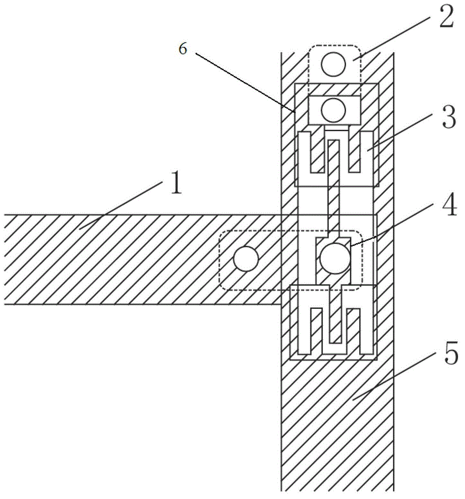
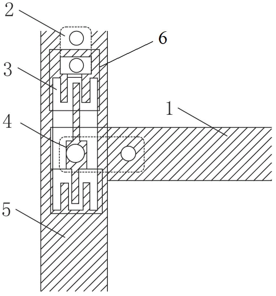
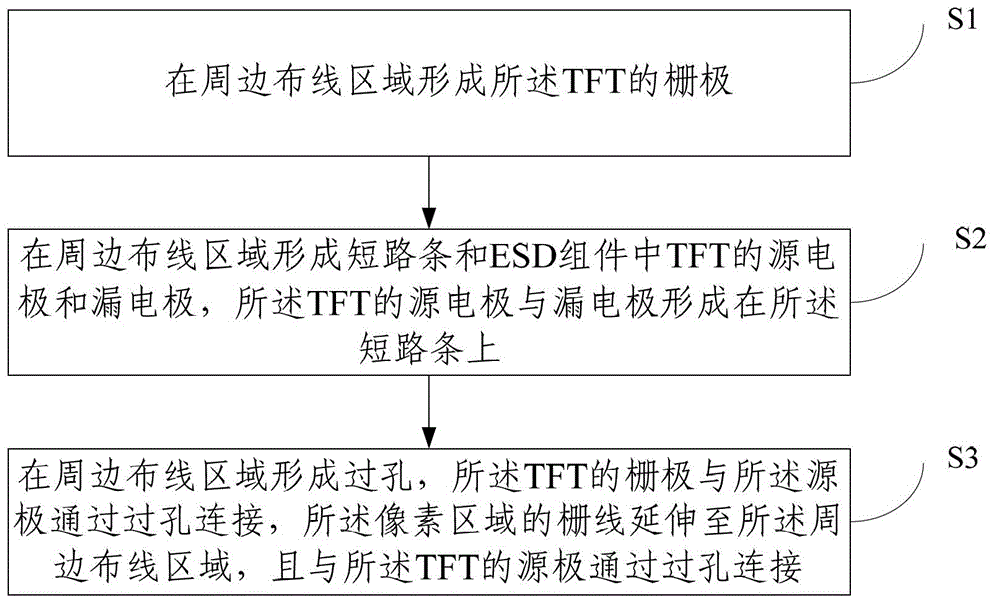
[0028] Embodiments of the present invention are described in detail below, examples of which are shown in the drawings, wherein the same or similar reference numerals designate the same or similar elements or elements having the same or similar functions throughout. The embodiments described below by referring to the figures are exemplary only for explaining the present invention and should not be construed as limiting the present invention.

[0029] In describing the present invention, it should be understood that the terms "center", "longitudinal", "transverse", "upper", "lower", "front", "rear", "left", "right", " The orientations or positional relationships indicated by "vertical", "horizontal", "top", "bottom", "inner", "outer", etc. are based on the orientation or positional relationships shown in the drawings, and are only for the convenience of describing the present invention and simplifying Describes, but does not indicate or imply that the device or element referred...


PUM


Abstract

The invention relates to the technical field of displaying, in particular to a display device, an array substrate and a fabrication method of the array substrate. The array substrate comprises a pixel zone and a peripheral wiring zone, wherein the peripheral wiring zone is provided with an ESD (Electro-Static Discharge) component and a short-circuiting strip; the ESD component comprises a plurality of TFTs (Thin Film Transistors); and source electrodes and drain electrodes of the TFTs are arranged on the short-circuiting strip. According to the display device, the array substrate and the fabrication method, as the source electrodes and the drain electrodes of the TFTs in the ESD component are arranged on the short-circuiting strip, the horizontal distance occupied by ESD devices on the two sides of a substrate display zone can be effectively shortened, the position of a whole peripheral circuit deviates towards the display zone, the distance between the display zone and a glass edge can be effectively shortened, the narrow frame performance of a display product can be better realized, and the market competitiveness of the product can be improved.

Description

technical field [0001] The present invention relates to the field of display technology, in particular to a display device, an array substrate and a preparation method thereof. Background technique [0002] In recent years, with the continuous development and improvement of TFT-LCD (Thin Film Transistor Liquid Crystal Display) liquid crystal display technology, the display performance of narrow borders has become more and more widely sought after by users. [0003] In the TFT-LCD manufacturing process, electrostatic protection is the key to the entire process control. In order to avoid the impact of static electricity on product quality, in the prior art, ESD (Electro-Static discharge, electrostatic discharge) components composed of reversely connected diodes are usually used to better protect against static electricity. [0004] However, since the installed anti-static ESD components need to occupy the space of the display area on the substrate, in this way, the display ar...

Claims


Application Information

Patent Timeline
Patent Type & Authority Applications(China)
IPC IPC(8): H01L27/02H01L29/786H01L21/77G02F1/1362G02F1/1368
CPCH01L27/1259H01L23/60H01L27/124H01L27/0296H01L2924/0002H01L2924/00
Inventor 于海峰封宾林鸿涛
Owner BOE TECH GRP CO LTD
Why Eureka
Try Eureka