Manufacturing method of substrate and manufacturing method of wiring substrate

A manufacturing method and substrate technology, which are applied in the field of substrate manufacturing and wiring substrate manufacturing, can solve problems such as metal ion concentration deviation, and achieve the effects of high connection reliability, avoiding deviation of metal filling degree, and improving productivity.

Inactive Publication Date: 2013-03-27
HOYA CORP
View PDF1 Cites 6 Cited by
  • Summary
  • Abstract
  • Description
  • Claims
  • Application Information

AI Technical Summary

Problems solved by technology

[0010] In addition, in the case of a substrate on which a plurality of through-holes 51 are formed, the concentration of metal ions tends to vary between areas where the distribution density of the through-holes 51 is sparse and areas where the distribution density is dense.

Method used


Image

  • Manufacturing method of substrate and manufacturing method of wiring substrate
  • Manufacturing method of substrate and manufacturing method of wiring substrate
  • Manufacturing method of substrate and manufacturing method of wiring substrate

Examples


no. 1 Embodiment approach )

[0059]

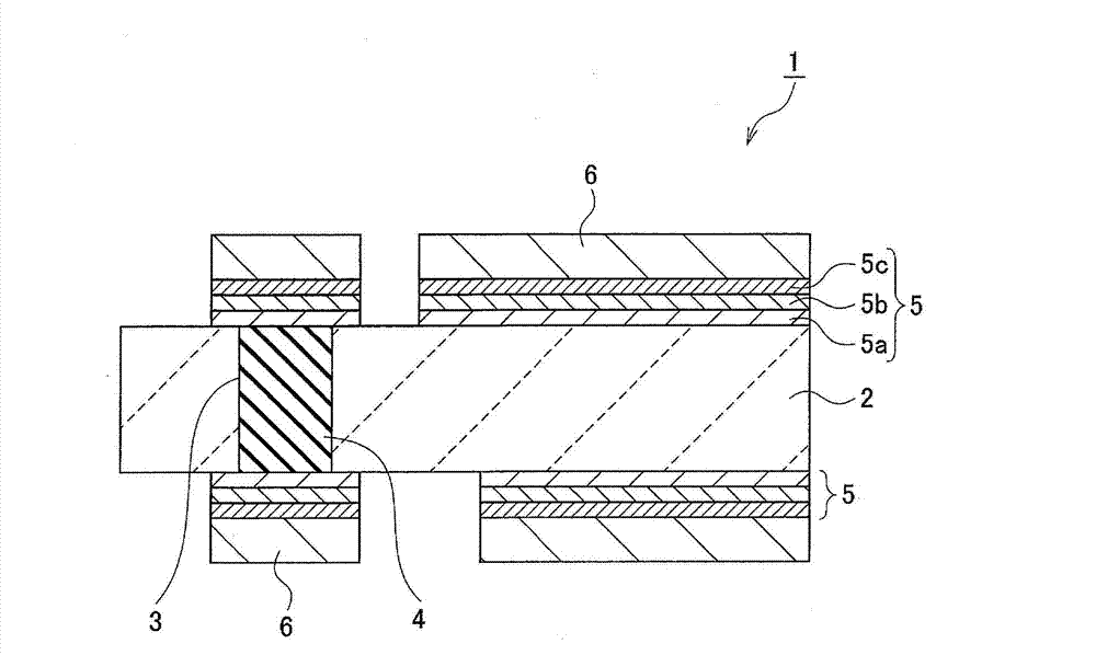
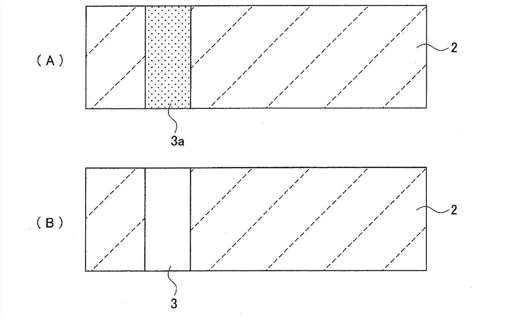
[0060] figure 1 It is a cross-sectional view showing a configuration example of the wiring board according to the embodiment of the present invention. The illustrated wiring board 1 is configured using a glass substrate 2 . The glass substrate 2 is used as a core substrate of the wiring substrate 1 . The glass substrate 2 is provided with multiple ( figure 1 Only 1 shown in ) through hole 3. Through hole 3 is filled with metal 4 . Wiring patterns 6 are formed on the first surface and the second surface of the glass substrate 2 via the adhesion layer 5 , respectively. Therefore, the wiring substrate 1 constitutes a double-sided wiring substrate. The first surface and the second surface of the glass substrate 2 are in a relationship of a front surface and a back surface. exist figure 1 Herein, the lower surface of the glass substrate 2 is defined as the first surface, and the upper surface of the glass substrate 2 is defined as the second surface. The wirin...

no. 2 Embodiment approach )

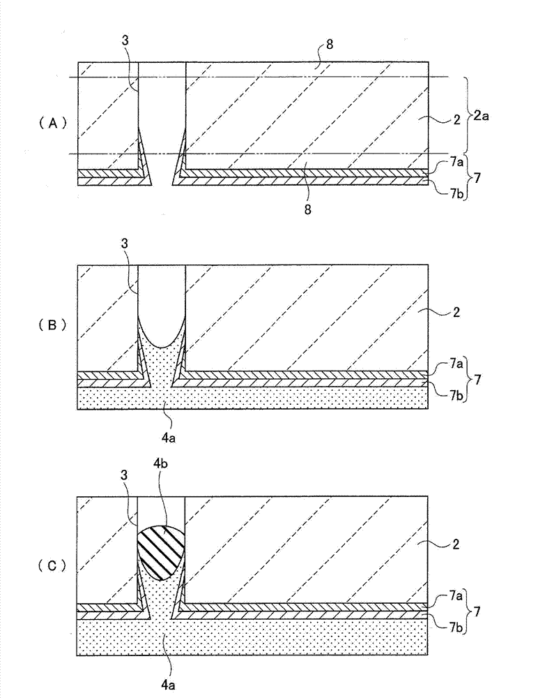
[0125] Hereinafter, the substrate manufacturing method and the wiring substrate manufacturing method according to the second embodiment of the present invention will be described based on the drawings. Figure 10 A flowchart showing the wiring board manufacturing method according to the present embodiment, Figure 8 It shows process diagrams from the plating base layer forming process S20 to the metal filling process S40. Additionally, if Figure 10 As shown in the flow chart of , the present embodiment differs from the first embodiment in that the fourth step (metal filling step S40 ) is divided into a planarization step S41 and a filling step S42 . The other steps are the same as those of the first embodiment, and therefore detailed descriptions are omitted.

[0126] The metal filling step S40 of this embodiment is as follows: Figure 8 As shown in (B), the surface inside the through-hole 3 of the first plating layer 4 a formed in the opening sealing step S30 (the second ...

no. 3 Embodiment approach )

[0159] This embodiment is as Figure 11 What is shown is an embodiment related to a method of manufacturing a substrate 2 in which the distribution density of the through-holes 3 has a sparse region 9a and a dense region 9b. First, the relationship between the formation state of the through-hole and the electrolytic plating, which is most relevant to the present embodiment, will be described. Among them, the substrate manufacturing method of this embodiment has the same Figure 10 The manufacturing process is the same as that of the second embodiment shown, and therefore detailed descriptions of the respective manufacturing processes are omitted.

[0160] In the present embodiment, a plurality of through-holes 3 to be filled with metal by electrolytic plating are provided on the glass substrate 2 . Furthermore, on the glass substrate 2, a region 9a in which the through-holes 3 are sparsely distributed and a region 9b in which the through-holes 3 are densely distributed are m...


PUM


Abstract

Provided are manufacturing methods of a substrate and a wiring substrate, including a step A of forming a primary plating layer on a lower side of a glass substrate having a through-hole; a step B of sealing a lower opening of the through-hole by forming a first layer on an upper side using electroplating; and a step C of filling the through-hole by depositing a second layer in the through-hole using electroplating from the upper side. In the step A, the primary plating layer is formed on from a lower opening edge to a partial sidewall surface of the through-hole. In the step B, the lower opening is sealed by growing the first layer from a primary plating layer surface inside the through-hole. In the step C, the through-hole is filled with plating metal by growing the second layer from a first layer surface inside the through-hole toward an upper opening.

Description

technical field [0001] The present invention relates to a substrate manufacturing method using a glass base material and a wiring substrate manufacturing method. Background technique [0002] In recent years, for example, for wiring boards on which electronic components such as MEMS (Micro Electro Mechanical System: Micro Electro Mechanical System) are mounted, high connection reliability can be ensured and electronic components can be mounted at high density. In response to this, the inventors of the present application have proposed a substrate manufacturing method in which a glass substrate excellent in smoothness, rigidity, insulation, heat resistance, etc. is used as a core for a wiring substrate instead of a resin substrate. The substrate can be used as a double-sided wiring substrate by filling metal through-holes formed in the glass substrate (for example, refer to Patent Document 1). [0003] Patent Document 1 proposes a substrate manufacturing method including a s...

Claims


Application Information

Patent Timeline
Patent Type & Authority Applications(China)
IPC IPC(8): H05K3/42H05K1/11
CPCC25D5/18H05K3/00H05K1/0306H05K3/002H05K3/0029H05K3/423H05K2201/09827H05K2201/09854H05K2203/025H05K2203/0733H05K2203/1476H05K2203/1572H05K3/40H05K1/03
Inventor 伏江隆菊地肇
Owner HOYA CORP
Why Eureka
Try Eureka