Sapphire epitaxial wafer structure and manufacturing method thereof

A manufacturing method, sapphire technology, applied in semiconductor devices, electrical components, circuits, etc., can solve problems such as lattice mismatch, achieve the effects of improving crystal quality, improving quantum luminous efficiency, and reducing stress

Active Publication Date: 2013-04-03
BYD SEMICON CO LTD
View PDF3 Cites 3 Cited by
  • Summary
  • Abstract
  • Description
  • Claims
  • Application Information

AI Technical Summary

Problems solved by technology

[0005] The present invention solves the problem of lattice mismatch caused by directly growing GaN on a sapphire substrate in the prior art, thereby providing a sapphire epitaxial wafer structure and a manufacturing method thereof that reduce lattice mismatch and defects

Method used


Image

  • Sapphire epitaxial wafer structure and manufacturing method thereof
  • Sapphire epitaxial wafer structure and manufacturing method thereof
  • Sapphire epitaxial wafer structure and manufacturing method thereof

Examples


Embodiment Construction

[0016] In order to make the technical problems, technical solutions and beneficial effects solved by the present invention clearer, the present invention will be further described in detail below in conjunction with the accompanying drawings and embodiments. It should be understood that the specific embodiments described here are only used to explain the present invention, not to limit the present invention.

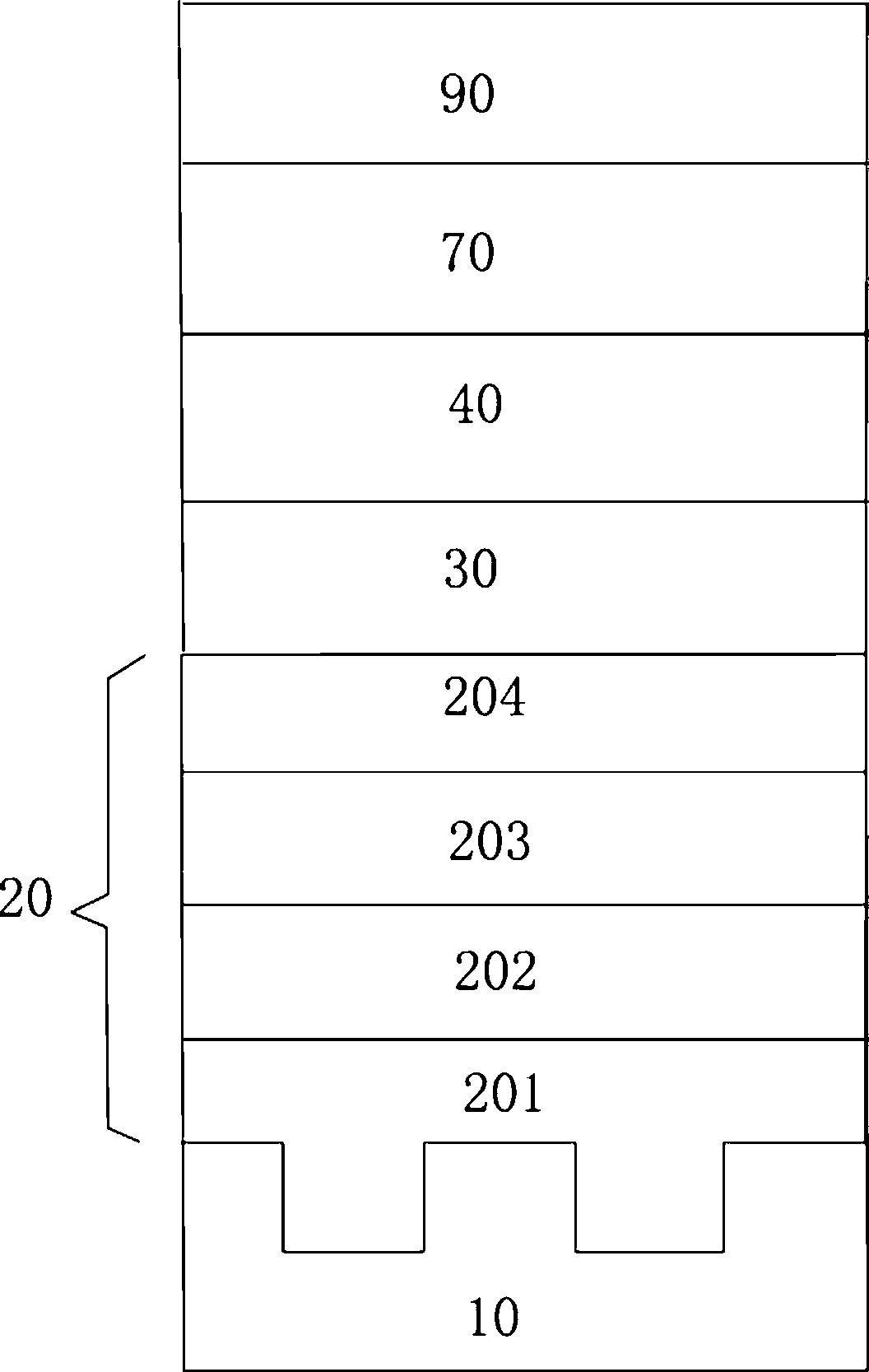
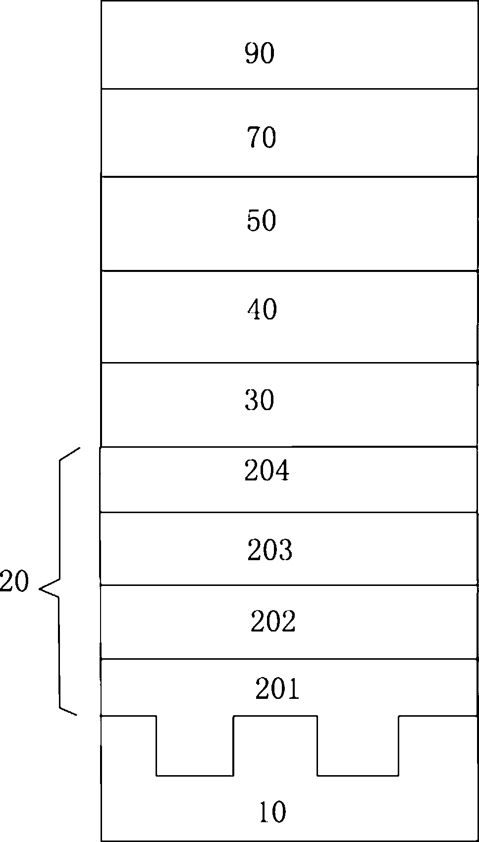
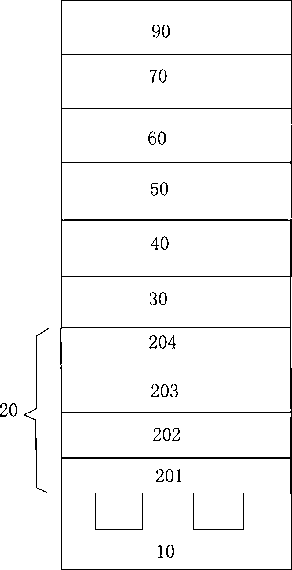
[0017] figure 1 It is a schematic diagram of the structure of a sapphire epitaxial wafer according to the first embodiment of the present invention, and discloses a structure of a sapphire epitaxial wafer, including: a sapphire substrate 10, a buffer layer 20 disposed on the sapphire substrate 10, and an intrinsic epitaxial wafer disposed on the buffer layer 20. GaN layer 30, N-type GaN layer 40 disposed on intrinsic GaN layer 30, MQW light-emitting layer 70 disposed on N-type GaN layer 40, P-type GaN layer 90 disposed on MQW light-emitting layer 70; wherein, the The bu...


PUM


Abstract

The invention provides a sapphire epitaxial wafer structure. The sapphire epitaxial wafer structure comprises a sapphire substrate, a buffer layer arranged on the sapphire substrate, an intrinsic GaN layer arranged on the buffer layer, an N-type GaN layer arranged on the intrinsic GaN layer, an MQW (Multiple Quantum Well) luminous layer arranged on the N-type GaN layer, and a P-type GaN layer arranged on the MQW luminous layer, wherein the buffer layer comprises a Ge-doped InN layer, a Ge-doped GaN layer, a first GaN layer and a second GaN layer which are sequentially arranged on the sapphire substrate, wherein the first GaN layer is formed at 500-600 DEG C, and the second GaN layer is formed at 1000-1100 DEG C. The invention also provides a manufacturing method of a sapphire epitaxial wafer; and a double-step epitaxial growth method is adopted for manufacturing the buffer layer, and a small amount of Ge is doped in InN of the buffer layer and spreads to InN gaps so that stress generated by the lattice mismatch between a sapphire and the GaN can be effectively reduced, and the luminous efficiency of a quantum is improved.

Description

technical field [0001] The invention relates to the technical field of semiconductor lighting devices, in particular to a sapphire epitaxial wafer structure and a manufacturing method thereof. Background technique [0002] As the third generation of lighting, LED lighting has the advantages of low power consumption, energy saving, environmental protection and long life, and GaN-based semiconductor materials in the third generation of semiconductor materials have attracted wide attention. Group III nitrides (III-V compounds) including GaN, InN, AlN and ternary and quaternary solid solutions are all direct bandgap wide bandgap materials, and their bandgap ranges from 0.7eV of InN to 6.28eV of AlN, GaN-based Semiconductor materials have become the material system with the widest band gap, and have been widely used in optoelectronic devices in blue, green, and ultraviolet bands. The quality of GaN crystal directly affects its luminous efficiency, so growing high-quality GaN has...

Claims


Application Information

Patent Timeline
Patent Type & Authority Applications(China)
IPC IPC(8): H01L33/12H01L33/00
Inventor 吴明驰
Owner BYD SEMICON CO LTD
Why Eureka
Try Eureka