Chip with scan chain test function and test method

A scanning chain and chip technology, applied in the direction of measuring electricity, measuring devices, measuring electrical variables, etc., can solve the problems that the circuit cannot be completely tested, reduce the scanning test coverage of the chip combination circuit, and cannot change the excitation signal, etc., to achieve reduction Effects of occupancy, increased coverage, time saved

Active Publication Date: 2013-04-10
SPREADTRUM COMM (SHANGHAI) CO LTD
View PDF4 Cites 24 Cited by
  • Summary
  • Abstract
  • Description
  • Claims
  • Application Information

AI Technical Summary

Problems solved by technology

[0015] It can be seen that in the prior art, a large number of chip pins need to be reused for test mode and function module parameter configuration during the chip scan test process, and these pins must always maintain a fixed value during the chip scan test process to maintain the set value. Therefore, during the functional test, the excitation signal of the combined circuit connected to these ...

Method used


Image

  • Chip with scan chain test function and test method
  • Chip with scan chain test function and test method
  • Chip with scan chain test function and test method

Examples


specific Embodiment 1

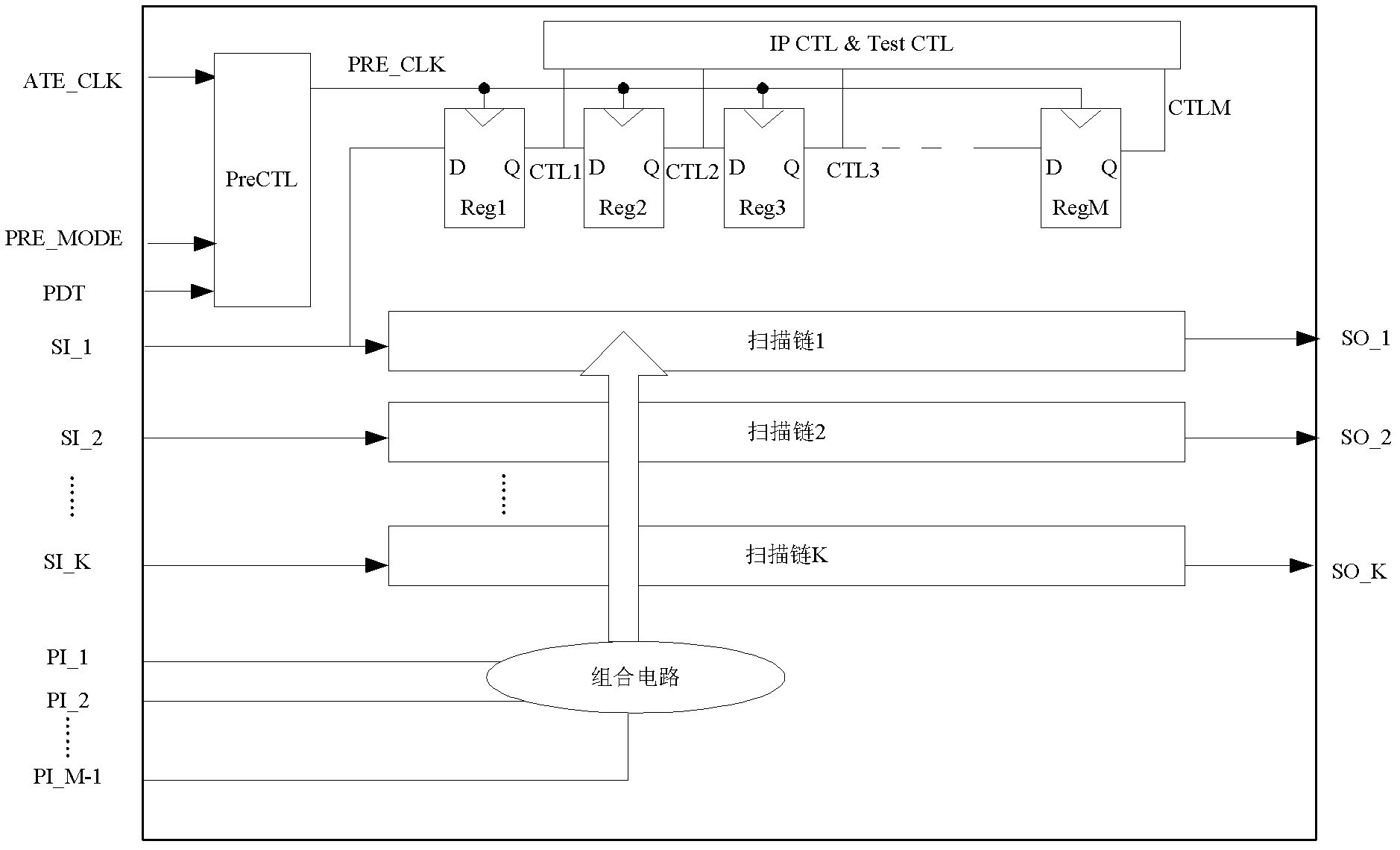
[0055] This embodiment is a preferred implementation of the chip with scan chain test function of the present invention, the specific structure is as follows image 3 shown, including:

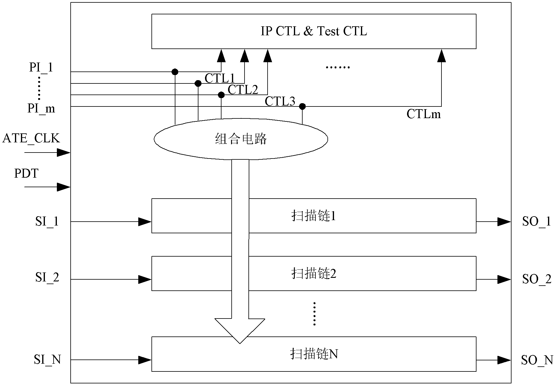
[0056] Test mode and function module parameter configuration module (IP CTL & Test CTL), combined circuit, multiple scan chains (for example, K scan chains, scan chain 1 to scan chain K); and:

[0057] The parameter latching trigger chain is composed of multiple (m) flip-flops (Reg1~Regm) connected in series, and is used to receive and latch test mode parameters and function module configuration parameters; the previous trigger in the trigger chain The data output terminal Q of the flip-flop is connected to the data input terminal D of the next flip-flop; the data output terminals of each flip-flop are respectively connected to the control value input terminals CTL1~CTLm of IP CTL & Test CTL; provide test mode for IP CTL & Test CTL And function module parameter control value; The clock input ...

specific Embodiment 2

[0070] This embodiment is a preferred implementation manner of the chip with scan chain testing function of the present invention.

[0071] The chip in this embodiment includes all the modules of the chip in Embodiment 1. At the same time, the data output end of the parameter latch flip-flop chain, that is, the data output end Q of the last flip-flop is also coupled to a pin of the chip.

[0072] In this way, after the parameter setting control module turns on the clock of each trigger of the parameter latch trigger chain, before configuring the test mode and function parameters, each trigger in the parameter latch trigger chain can be tested. The specific test method is: Under the control of the scan clock, the test vectors are moved into the parameter latching flip-flop chain one by one through the chip pins connected to the data input end of the first flip-flop in the parameter latching flip-flop chain, and the last flip-flop in the parameter latching flip-flop chain The ou...

specific Embodiment 3

[0077] This embodiment is a preferred implementation of the chip testing method with scan chain testing function of the present invention, the specific process is as follows Figure 8 shown, including:

[0078] 1. The parameter setting control module outputs the scan clock signal to each trigger clock input end of the parameter latch trigger chain;

[0079] 101. Set the PDT pin of the chip to 1 (valid), and enter the scan test;

[0080] 102. Set the pin connected to PRE_MODE to 1 (valid), and the parameter setting control module outputs the scan clock signal to each trigger clock input end of the parameter latch trigger chain through PRE_CLK;

[0081] 2. Under the control of the scan clock, the test mode and the parameter control value of the function module are serially moved into each flip-flop of the parameter latch flip-flop chain;

[0082] 3. The parameter setting control module closes the scan clock signal output, and each trigger output terminal of the parameter latch...


PUM


Abstract

The invention discloses a chip with a scan chain test function. The chip comprises a plurality of scan chains, a combination circuit, a test mode and function module parameter configuration module, a parameter latch trigger chain formed by connecting a plurality of triggers in series and a parameter setting control module. Test mode and function module parameter control words are moved into the trigger chain under the control of the parameter setting control module and latched to the output end of each trigger to provide control value for the test mode and function module parameter configuration module to configure test mode and function module parameter. A corresponding test method is further disclosed. By means of the technical scheme, the chip can effectively improve test covering rate of the combination circuit of the chip and reduce occupation of pins in a chip scanning test.

Description

technical field [0001] The invention relates to chip testing technology, in particular to a chip with scan chain testing function and a testing method. Background technique [0002] In the field of System on Chip (SOC) chip test, scan test is the most basic and most important test item. [0003] The structure of the scan chain is attached figure 1 As shown, the data input terminal of the register REG is connected to the scan data input (short for, scan_in) or combinational circuit through the selector MUX under the control of the scan_enable control signal; in the scan shift mode, the data input terminal D of the register is connected to scan_in , the output terminal Q of the previous register in the scan chain is used as the scan_in of the latter register. The scan_in of the first register of the scan chain is connected to the scan data input pin SI of the scan chain, and the Q terminal of the last register is connected to the scan data output pin SO of the scan chain; in...

Claims


Application Information

Patent Timeline
IPC IPC(8): G01R31/3185
Inventor 邱远贾伟唐明熊洋
Owner SPREADTRUM COMM (SHANGHAI) CO LTD
Why Eureka
Try Eureka