Interposer, circuit board module, and method for manufacturing interposer

A technology for inserts and circuit boards, which is applied in the fields of printed circuit manufacturing, electrical component assembly of printed circuits, semiconductor/solid-state device manufacturing, etc. It can solve problems such as misalignment, unsuitable alignment, and through-hole inclination.

Inactive Publication Date: 2013-04-10
FUJITSU LTD
View PDF4 Cites 0 Cited by
  • Summary
  • Abstract
  • Description
  • Claims
  • Application Information

AI Technical Summary

Problems solved by technology

[0012] However, this structure is not suitable for the alignment of the lower contact to the lower contact along the vertical direction (Z direction).
Misalignment in the Z direction skews the via, resulting in misalignment of the upper contact in the X-Y direction

Method used


Image

  • Interposer, circuit board module, and method for manufacturing interposer
  • Interposer, circuit board module, and method for manufacturing interposer
  • Interposer, circuit board module, and method for manufacturing interposer

Examples


Embodiment Construction

[0025] specific implementation plan

[0026] Embodiments will now be described with reference to the drawings.

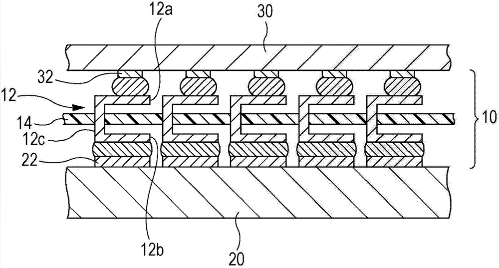
[0027] figure 1 is a schematic diagram of the electrode structure of an interposer according to one embodiment. The interposer 10 is an intermediate substrate disposed between the circuit board 20 and the semiconductor device 30 which is an electronic component having a plurality of electrodes. The interposer 10 includes a plurality of spring electrodes 12 and a substrate 14 holding the spring electrodes 12 . The spring electrodes 12 are soldered to the electrode pads 22 of the circuit board 20 and the electrodes 32 of the semiconductor device 30 . That is, the electrodes 32 of the semiconductor device 30 are connected to the electrode pads 22 of the circuit board 20 via the spring electrodes 12 . Thus, the semiconductor 30 is mounted and fixed to the circuit board 20 .

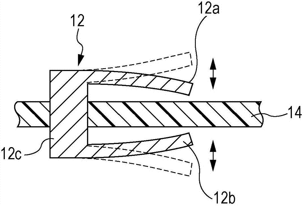
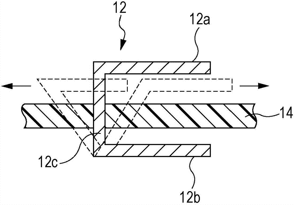
[0028] The spring electrodes 12 are U-shaped electrodes each including an upper pad 12a, a...


PUM


Abstract

The invention relates to an interposer, a circuit board module, and a method for the manufacturing interposer. The interposer includes a substrate having first and second opposing surfaces, the substrate having a sheet shape; and a plurality of spring electrodes fixed to the substrate in a certain arrangement, each of the plurality of the spring electrodes including a first pad disposed opposite the first surface of the mesh and extending in a first direction, a second pad disposed opposite the second surface of the mesh and extending in the first direction, and a post extending through the substrate between the first and second surfaces and connecting an end of the first pad to an end of the second pad.

Description

technical field [0001] Embodiments discussed herein relate to mounting structures for mounting electronic components on circuit boards. Background technique [0002] The circuit board module is assembled by mounting electronic parts such as semiconductor devices on a printed circuit board. A mounting structure is proposed to ensure that the circuit board module has sufficient connection reliability against thermal stress occurring in the mounting structure and strain due to impact. For example, a common structure strengthens the solder joint between the electronic component and the printed circuit board by filling the space between the electronic component and the printed circuit board (beneath the electronic component) with a filler such as an adhesive. Also available is a resin sealing structure that completely covers electronic components soldered to a printed circuit board with a sealing resin. [0003] The use of fillers and encapsulation resins enables rigid attachme...

Claims


Application Information

Patent Timeline
Patent Type & Authority Applications(China)
IPC IPC(8): H01L23/485H05K3/32H01L21/60
CPCH01L23/145H01L23/49811H01L24/16H01L2224/16235H01L2224/16238H01L2924/351H05K1/0366H05K3/0014H05K3/3436H05K3/4092H05K2201/0154H05K2201/0162H05K2201/0311H05K2201/09118H05K2201/09563H05K2201/10378H05K2201/10962Y10T29/49155Y02P70/50H01L2924/00H01L23/12H01R11/01H05K3/32
Inventor 森谷康雄
Owner FUJITSU LTD
Why Eureka
Try Eureka