Interposer, method of fabricating the same, and semiconductor device using the same

a technology of interposers and semiconductor devices, applied in semiconductor devices, semiconductor/solid-state device details, electrical apparatus, etc., can solve the problems of increasing cost, increasing the size of the interposer, and difficulty in forming wiring patterns, so as to reduce the cost of the interposer

Active Publication Date: 2006-01-05
SHINKO ELECTRIC IND CO LTD
View PDF17 Cites 124 Cited by
  • Summary
  • Abstract
  • Description
  • Claims
  • Application Information

AI Technical Summary

Benefits of technology

[0012] An object of the present invention is to provide an interposer w

Problems solved by technology

In particular, where a chip having a large number of terminals is to be mounted, the size of the interposer becomes even larger.
Accordingly, there has been the following problem: where an interposer is fabricated using only silicon (Si), Si needs to be used even for an area which is essentially unnecessary from the vi

Method used


Image

  • Interposer, method of fabricating the same, and semiconductor device using the same
  • Interposer, method of fabricating the same, and semiconductor device using the same
  • Interposer, method of fabricating the same, and semiconductor device using the same

Examples


Embodiment Construction

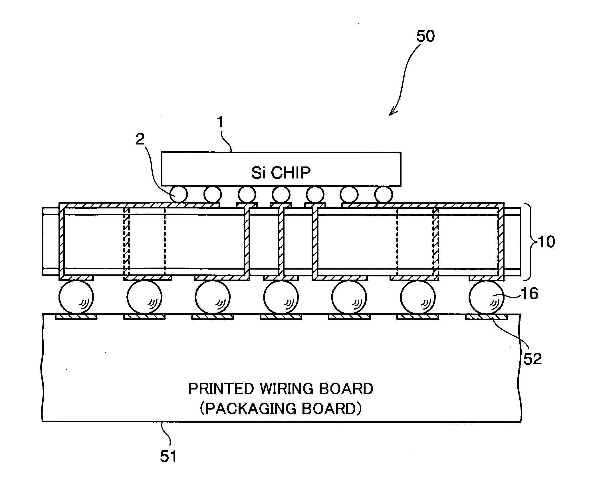
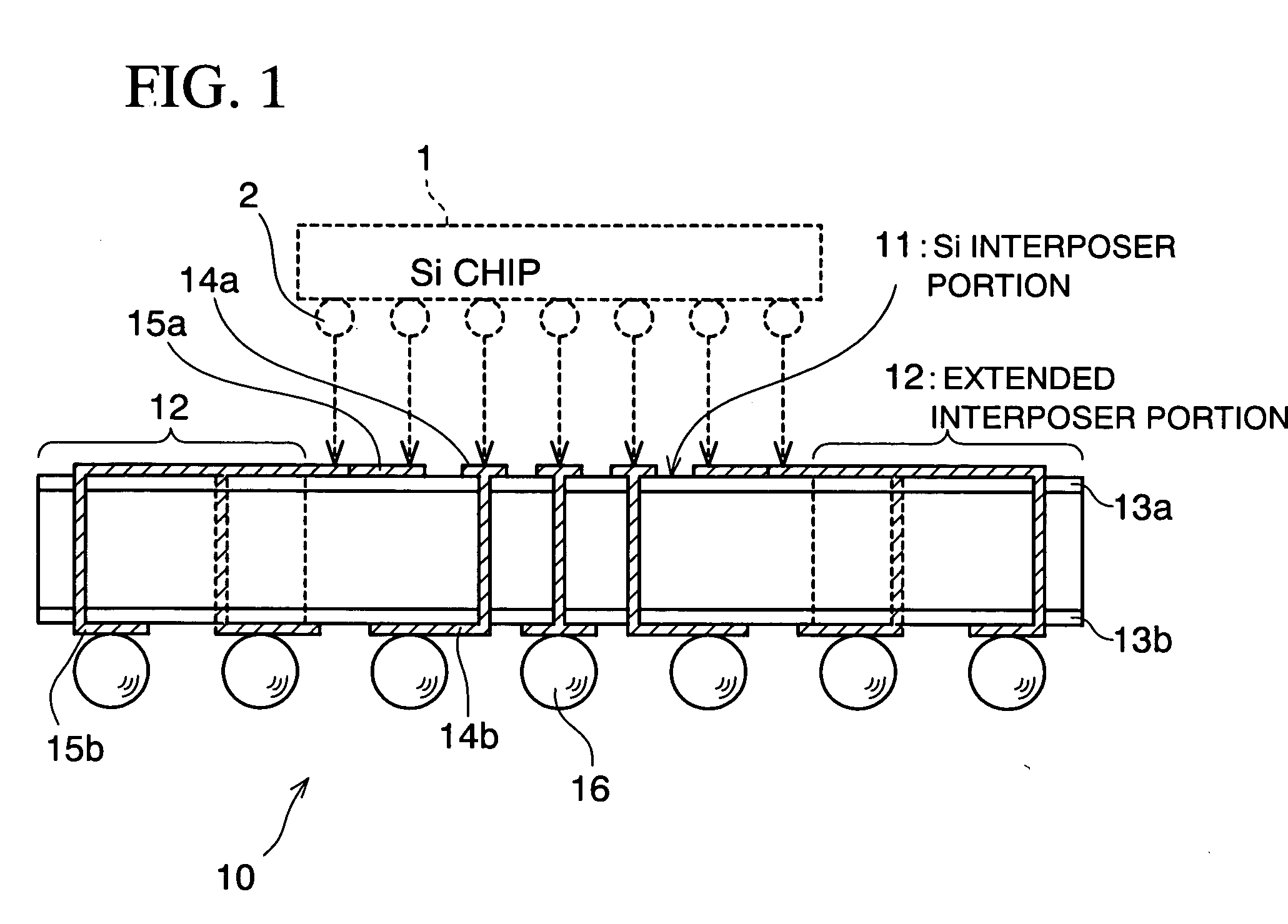
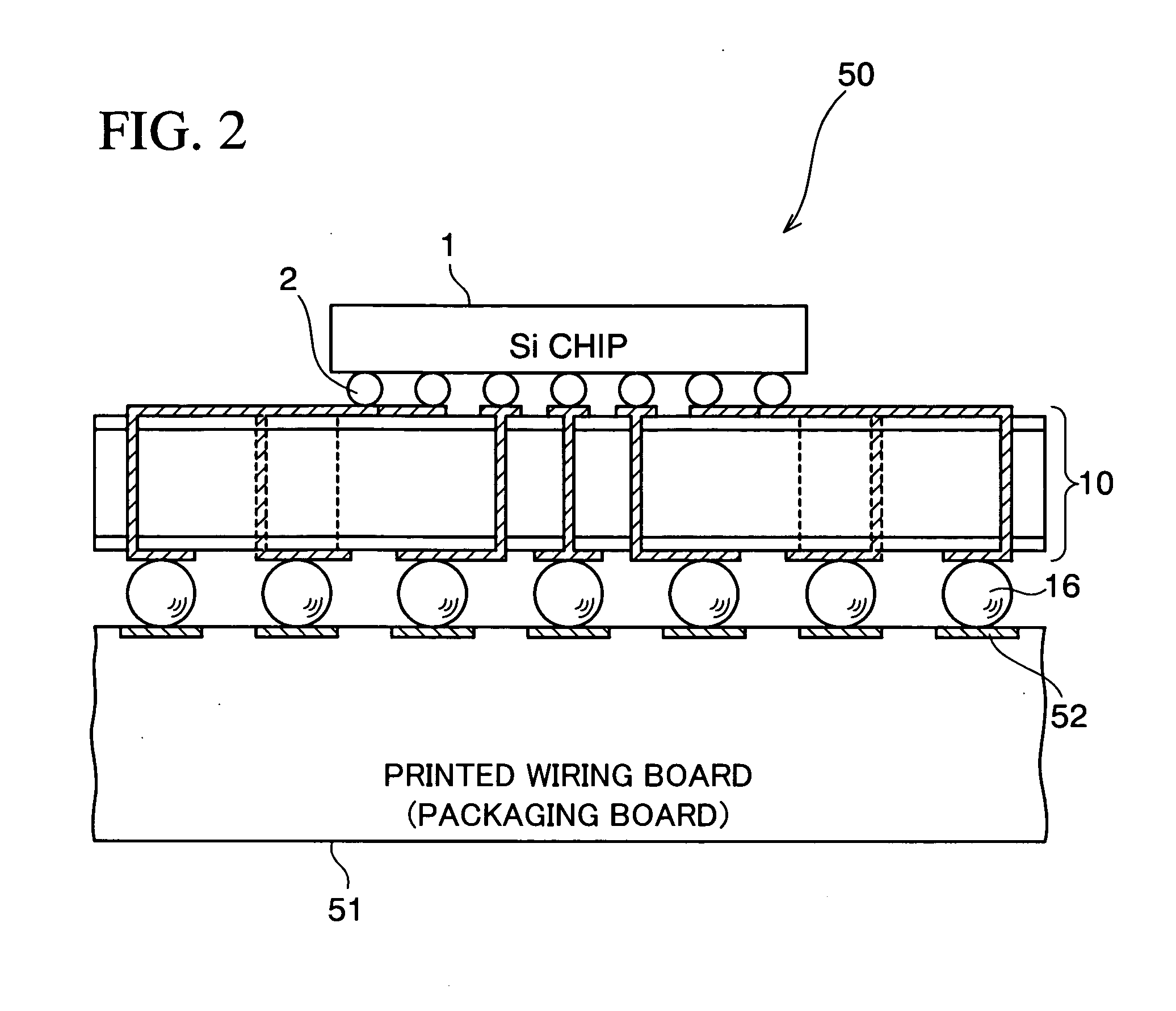
[0032]FIG. 1 schematically shows, in a cross-sectional view, the constitution of an interposer according to one embodiment of the present invention. In the illustrated example, in order to clearly show the portions relating to the present invention, the constitution of the interposer is shown in a simplified manner. The detailed constitution (structure) thereof will be described later in conjunction with the process.

[0033] On the interposer 10 according to this embodiment, a silicon (Si) chip 1 is mounted as indicated by dashed lines in the drawing. As described later, the interposer 10 with the Si chip 1 mounted thereon is mounted on a packaging board to constitute a semiconductor device. The interposer 10 has, as its basic structure, a portion 11 (hereinafter referred to as a “Si interposer portion”) which is made of Si necessary for matching its coefficient of thermal expansion (CTE) with that of the Si chip 1 to be mounted thereon, and a portion 12 (hereinafter referred to as a...


PUM

PropertyMeasurementUnit
Temperatureaaaaaaaaaa
Sizeaaaaaaaaaa
Areaaaaaaaaaaa

Abstract

An interposer to be interposed between a semiconductor chip to be mounted thereon and a packaging board has an interposer portion made of a semiconductor and an interposer portion provided around the foregoing interposer portion integrally therewith. On both surfaces of the interposer portions, wiring patterns are formed via insulating layers. The wiring patterns are electrically connected via through holes formed at required positions in the interposer portions. The outer interposer portion is made of an insulator or a metal body. Further, external connection terminals are bonded to one surface of the interposer.

Description

CROSS-REFERENCE TO RELATED APLICATIONS [0001] This application is based on and claims priority of Japanese Patent Application No. 2004-193490 filed on Jun. 30, 2004, the entire contents of which are incorporated herein by reference. BACKGROUND OF THE INVENTION [0002] (a) Field of the Invention [0003] The present invention relates to an interposer for a semiconductor device, more particularly, to an interposer adapted to realize a required fan-out structure between a semiconductor chip to be mounted thereon and a printed wiring board (packaging board) such as a mother board. The present invention also relates to a method of fabricating the interposer, and a semiconductor device using the same. [0004] Such an interposer has a function of mounting a semiconductor chip thereon, and is therefore the same as a wiring board in terms of function and also referred to as a “package.”[0005] (b) Description of the Related Art [0006] A typical interposer has a semiconductor chip (typically a sil...

Claims


Application Information

Patent Timeline
IPC IPC(8): H01L21/48H01L23/52
CPCH01L21/6835Y10T29/49144H01L23/147H01L23/3677H01L23/492H01L23/49827H01L25/0657H01L2225/06517H01L2225/0652H01L2225/06541H01L2225/06572H01L2924/01078H01L2924/01079H01L2924/09701H01L2924/15311H01L2924/15331H01L2924/3511H01L2224/16225H01L2924/10253H01L23/14Y10T29/49165Y10T29/49117Y10T29/49155Y10T29/49126H01L2924/00H01L2924/00011H01L2924/00014H01L2224/0401
Inventor FUKASE, KATSUYAWAKABAYASHI, SHINICHI
Owner SHINKO ELECTRIC IND CO LTD
Why Eureka
Try Eureka