Semiconductor memory device and manufacturing method thereof

a memory device and semiconductor technology, applied in semiconductor devices, semiconductor/solid-state device details, instruments, etc., can solve the problems of physical limitation of memory cells, affecting the operation speed of the device, and reducing yield

Inactive Publication Date: 2009-12-03
LONGITUDE LICENSING LTD
View PDF20 Cites 123 Cited by
  • Summary
  • Abstract
  • Description
  • Claims
  • Application Information

AI Technical Summary

Benefits of technology

[0012]In the present invention, the core chips are mounted on the second surface of the interposer chip whenever desired. Therefore, productions of various specifications can be easily provided. More specifically, appropriate interface chips that the customers have select are mounted on the semiconductor memory devices, thus easily providing semiconductor memory devices. The core chips do not need to be stocked in the form of bare chips, in great quantities. It is therefore possible to flexibly manufacture semiconductor memory devices on demand to meet the customers' needs, while suppressing the degradation of reliability of the products.
[0015]Preferably, the pitch of the first through electrodes is substantially equal to the pitch of the first internal electrodes and the pitch of the second internal electrodes. If so, the wires can be less guided on the re-wiring layer.

Problems solved by technology

However, the miniaturization of memory cells is physically limited, and the increase in chip size leads to a reduction of yield and impairs an increase of operating speed.
Thus, the device can greatly increase the band width of signals to supply and receive to and from logic circuits such as CPUs that operate at high speed, although unable to perform large-scale parallel processing in corporation with the memory cores such as DRAMs that operate at low speed.
Inevitably, they cannot be flexibly manufactured on demand to meet the customers' needs.
However, this method is disadvantageous in that bare chips, i.e., chips not encapsulated yet, possibly remain long exposed to external conditions.
In particular, core chips probably become defective if exposed to the external conditions for a long time.
If they are stocked in large quantities and not encapsulated, they may degrade the reliability of the semiconductor memory devices, i.e., final products incorporating them.

Method used


Image

  • Semiconductor memory device and manufacturing method thereof
  • Semiconductor memory device and manufacturing method thereof
  • Semiconductor memory device and manufacturing method thereof

Examples


first embodiment

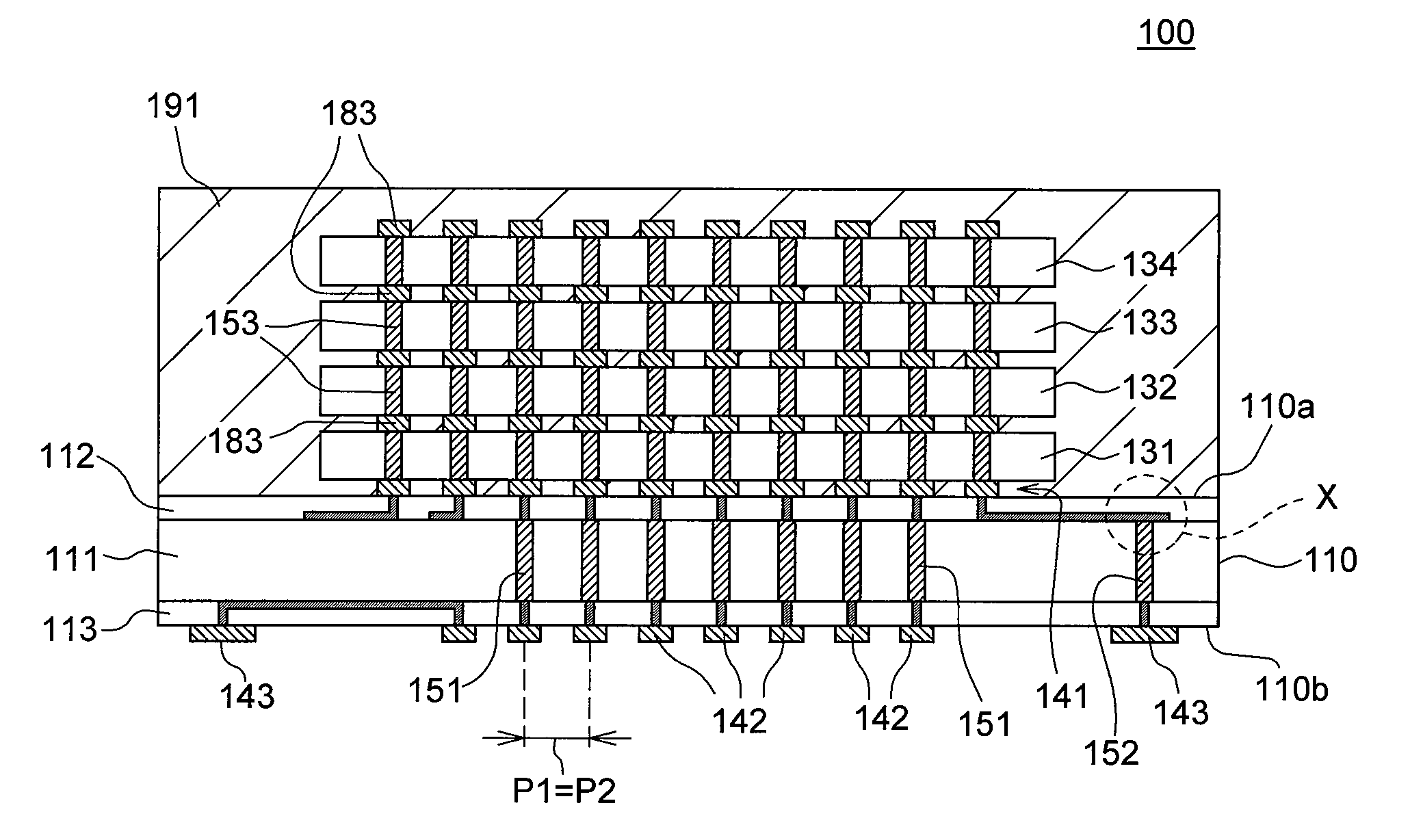
[0037]FIG. 1 is a sectional view of a semiconductor memory device 100 according to the present invention.

[0038]As shown in FIG. 1, the semiconductor memory device 100 according to the present invention has an interposer chip 110 and core chips (four core chips, in this example) 131 to 134. The core chips 131 to 134 are mounted one above another, on a core-mounting surface 110a (first surface) of the interposer chip 110. The core chips 131 to 134 mounted on the core-mounting surface 110a are molded with an encapsulating resin layer 191.

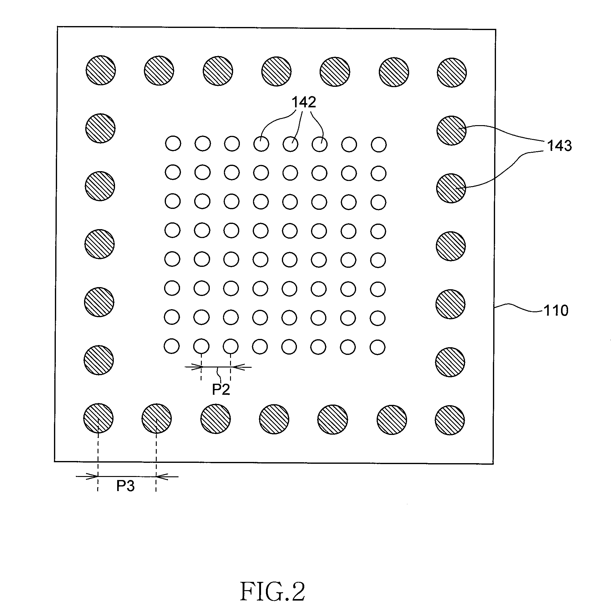
[0039]On the core-mounting surface 110a of the interposer chip 110 there are formed first internal electrodes 141. On a core-mounting surface 110b (second surface) of the interposer chip 110, there are formed second internal electrodes 142 and third internal electrodes 143. As shown in FIG. 2, which is a plan view of the interposer chip 110 as viewed from the mounting surface 110b, the second internal electrodes 142 are arranged on a central part of th...

second embodiment

[0069]FIG. 16 is a sectional view showing a semiconductor memory device 300 according to the present invention.

[0070]The semiconductor memory device 300 according to this embodiment differs from the semiconductor memory device 100 described above, in two respects. First, the interpose chip 110 has no component equivalent to the re-wiring layer 112. Second, all re-wiring is provided on the re-wiring layer 113. Because of these different features, the first internal electrodes 141 and the third internal electrodes 143 are aligned as viewed in the vertical direction, by using the re-wiring layer 113. Hence, in the present embodiment, the pitch of the first through electrodes 151 and the pitch of the second through electrodes 152 are substantially equal to the pitch of the first internal electrodes 141. Although not shown in FIG. 16, the re-wiring layer 113 connects the second internal electrodes 142 to the third internal electrodes 143, as in the first embodiment.

[0071]All re-wiring is...

third embodiment

[0072]FIG. 17 is a sectional view showing a semiconductor memory device 400 that is the present invention.

[0073]The semiconductor memory device 400 according to the third embodiment differs in one respect from the semiconductor memory device 300 according to the second embodiment. That is, the first through electrodes 151 and the second internal electrodes 142 are not connected in the same plane. Rather, the second internal electrodes 142 are guided by the re-wiring layer 113 and are thereby adjusted in position. In the third embodiment, the first internal electrodes 141 and the second internal electrodes 142 do not need to be aligned as viewed in the vertical direction. Thus, the interface chip 120 connected to the second internal electrodes 142 can be a general-purpose ASIC or the like, not a special ASIC that has electrodes arranged in specific positions. Furthermore, the re-wiring layer 113 can serve not only to adjust the second internal electrodes 142 in position, but also to ...


PUM


Abstract

A semiconductor memory device has a plurality of core chips and an interface chip, whose specification can be easily changed, while suppressing the degradation of its reliability. The device has an interposer chip. First internal electrodes connected to core chips are formed on the first surface of the interposer chip. Second internal electrodes connected to an interface chip and third internal electrodes connected to external electrodes are formed on the second surface of the interposer chip. The interface chip can be mounted on the second surface of the interposer chip whenever desired. Therefore, the memory device can have any specification desirable to a customer, only if an appropriate interface chip is mounted on the interposer chip, as is demanded by the customer. Thus, the core chips do not need to be stocked in great quantities in the form of bare chips.

Description

TECHNICAL FIELD[0001]The present invention relates to a semiconductor memory device and a manufacturing method thereof. More particularly, the invention relates to a semiconductor memory device in which a core unit having memory cells is integrated independently of an interface unit, and to a method of manufacturing a semiconductor memory device of this type.BACKGROUND OF THE INVENTION[0002]In recent years, the storage capacity of semiconductor memory devices, represented by a DRAM (Dynamic Random Access Memory), has increased. It is increasingly demanded that these devices can operate at higher speeds. The increase in storage capacity has been achieved by making memory cells smaller and by increasing the chip size. However, the miniaturization of memory cells is physically limited, and the increase in chip size leads to a reduction of yield and impairs an increase of operating speed.[0003]To solve these problems fundamentally, there has been proposed a method such that a core unit ...

Claims


Application Information

Patent Timeline
Patent Type & Authority Applications(United States)
IPC IPC(8): H01L23/52
CPCG11C5/02G11C5/025H01L24/97H01L2224/97H01L2224/94H01L21/6835H01L23/481H01L25/0657H01L25/50H01L2224/16145H01L2225/06513H01L2225/06517H01L2225/06527H01L2225/06541H01L2225/06555H01L2225/06572H01L2225/06586H01L2225/06596H01L2924/15311H01L2924/1532H01L2924/30105H01L2224/16225H01L2224/81005H01L2224/81H01L2924/15787H01L2224/05573H01L2224/13025H01L2924/00014H01L2924/181H01L2224/06131H01L2924/00H01L2224/05599H01L2924/00012
Inventor ISHINO, MASAKAZUIKEDA, HIROAKISHIBATA, KAYOKO
Owner LONGITUDE LICENSING LTD
Why Eureka
Try Eureka