Semiconductor memory with gate at least partially located in recess defined in vertically oriented semiconductor layer

a semiconductor layer and semiconductor technology, applied in the field of semiconductor memory, can solve the problems of inability to meet the requirements of reliability, difficult to write and erase, and limited thinning of gate insulating film, etc., and achieve the effect of increasing capacitance, high speed operation, and increasing the electrical field from the control gate to the active region of the memory cell

Inactive Publication Date: 2005-08-23
SAMSUNG ELECTRONICS CO LTD +1
View PDF19 Cites 86 Cited by
  • Summary
  • Abstract
  • Description
  • Claims
  • Application Information

AI Technical Summary

Benefits of technology

[0044]The present invention has been made in view of the above-mentioned problems and the following objects are intended. That is, according to the present invention, a semiconductor memory is constructed such that an electric field transmitting from the control gate to the active region of the memory cell is enhanced instead of increasing capacitance between the charge storage layer and the control gate. Device characteristics which allow high speed operation are obtained and an influence of the back-bias effect on the semiconductor memory having the charge storage layer and the control gate is reduced in order to achieve higher integration. The capacitance between the charge storage layer and the control gate is enlarged without increasing an area occupied by the memory cells. Variations in gate lengths of the memory cell transistors during the formation thereof are minimized to suppress variations in characteristics of the memory cells. The height of the island-like semiconductor layers is set smaller so that the island-like semiconductor layers are easily provided by forming a trench by etching. The open area ratio during the etching for forming the trench is reduced without increasing the area occupied by the memory cells, so that the island-like semiconductor layers are formed in an almost vertical direction with respect to the semiconductor substrate. Finally, itinerancy of thermal history of the memory cell transistors is minimized, thereby obtaining the semiconductor memory capable of suppressing variations in characteristics of the memory cells.

Problems solved by technology

That is, the larger the capacity between the floating gate and the control gate, the more effectively the potential of the control gate can be transmitted to the floating gate and the easier the writing and erasure become.
However, the thinning of the gate insulating film is limited in view of reliability of memory cells.
This is also questionable in view of reliability and is not practical.
This is, however, contradictory to the size reduction of memory cells and the capacity increase of EEPROM.
The selection gate lines can be formed continuously in self-alignment, but this is more difficult than the control gates 8 of the memory cells.
For, it is hard to form the diffusion layers selectively on the sidewalls of the pillar-form silicon layers.
Therefore, the production of mass-storage memories is difficult to realize.
The problem that the thresholds of memory cells are changed owing to a back-bias effect is true not only of the case where a plurality of memory cells are connected in series on one pillar-form semiconductor layer but also of the case where one memory cell is formed on one pillar-form semiconductor, depending upon variations in the back-bias effect of the substrate in an inplanar direction.
Therefore, it is difficult to increase the capacity between the charge storage layers and the control gates without increasing the area occupied by the memory cells.
In other words, it is difficult to increase the ratio of the capacity between the floating gates and the control gates to the capacity between the floating gates and the pillar-form semiconductor layers without increasing the area occupied by the memory cells.

Method used


Image

  • Semiconductor memory with gate at least partially located in recess defined in vertically oriented semiconductor layer
  • Semiconductor memory with gate at least partially located in recess defined in vertically oriented semiconductor layer
  • Semiconductor memory with gate at least partially located in recess defined in vertically oriented semiconductor layer

Examples


production example 1

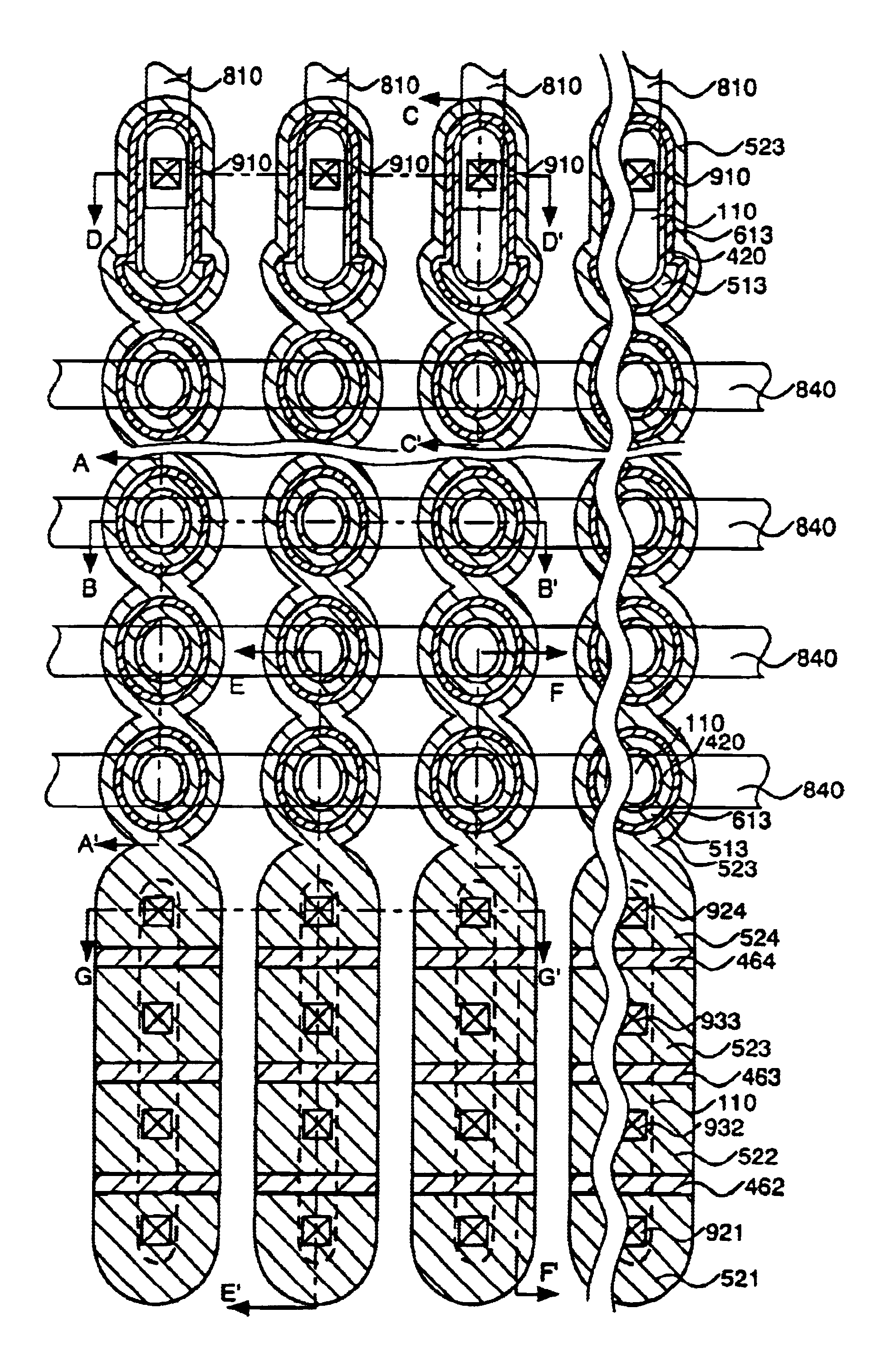
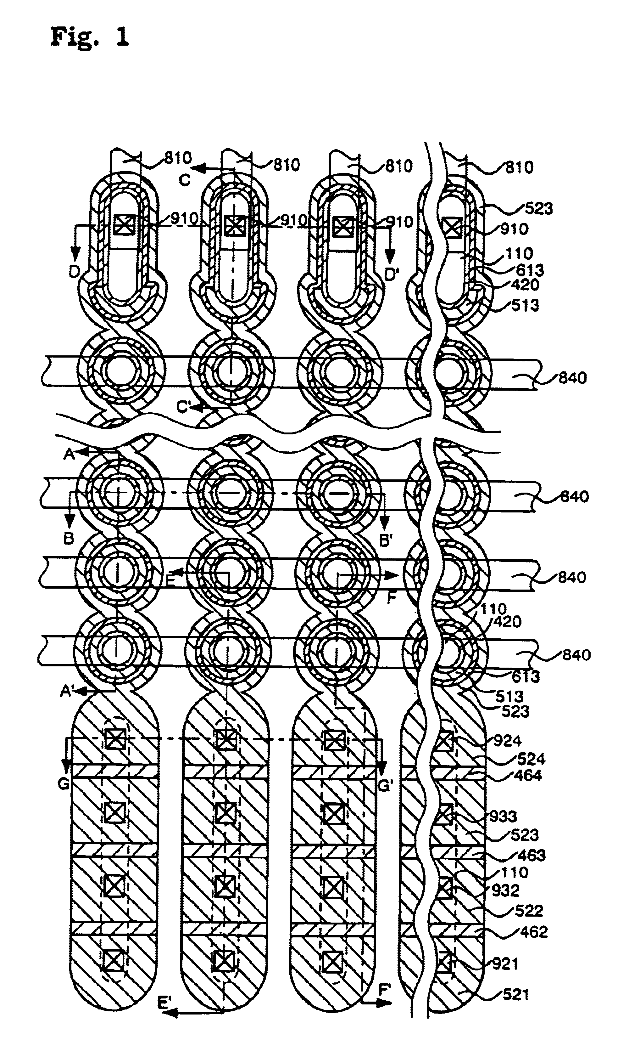
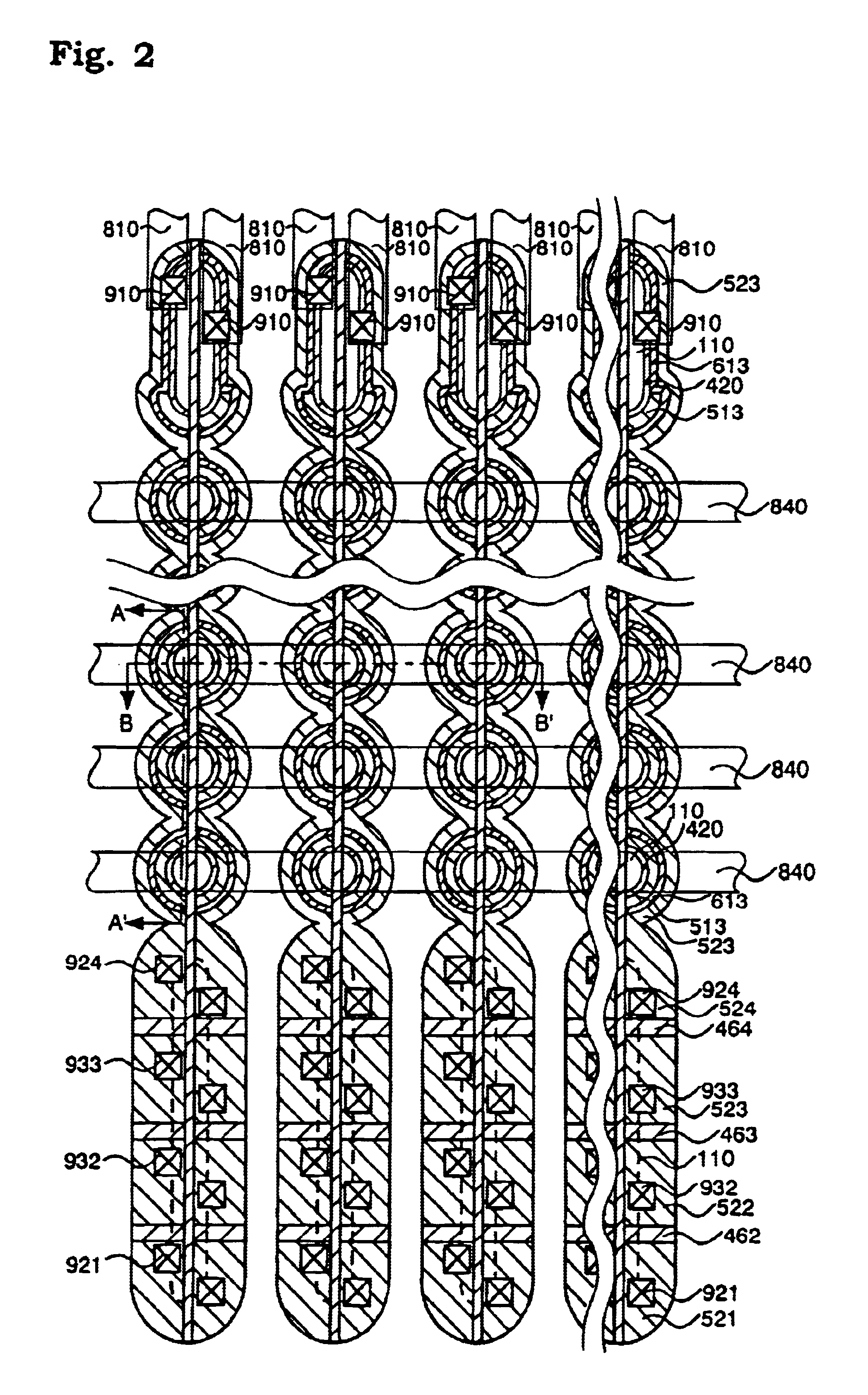
[0209]In a semiconductor memory to be produced in this example, a semiconductor substrate is patterned in the form of pillars to form island-like semiconductor layers having at least one recess. Sides of the island-like semiconductor layers make active regions. Tunnel oxide films, floating gates and control gates are formed in the recesses. The island-like semiconductor layers have additional recesses at the top and the bottom thereof and selection gate transistors including gate oxide films and selection gates are arranged therein. A plurality of memory transistors, for example, two memory transistors, are placed between the selection gate transistors and are connected in series along the island-like semiconductor layer. The thickness of gate insulating films of the selection gate transistors is larger than the thickness of gate insulating films of the memory transistors. The tunnel oxide films and the floating gates of the memory transistors are formed at the same time.

[0210]Such ...

production example 2

[0252]In a semiconductor memory to be produced in this example, a semiconductor substrate is patterned in the form of pillars to form island-like semiconductor layers having at least one recess. Sides of the island-like semiconductor layers make active regions. Tunnel oxide films, floating gates and control gates are formed in the recesses. The island-like semiconductor layers have additional recesses at the top and the bottom thereof and selection gate transistors including gate oxide films and selection gates are arranged therein. A plurality of memory transistors, for example, two memory transistors, are placed between the selection gate transistors and are connected in series along the island-like semiconductor layer. The thickness of gate insulating films of the selection gate transistors is larger than the thickness of gate insulating films of the memory transistors. The tunnel oxide films and the floating gates of the memory transistors are formed at the same time.

[0253]A sem...

production example 3

[0257]In a semiconductor memory to be produced in this example, a semiconductor substrate is patterned in the form of pillars to form island-like semiconductor layers having at least one recess. Sides of the island-like semiconductor layers make active regions. Tunnel oxide films, floating gates and control gates are formed in the recesses. The island-like semiconductor layers have additional recesses at the top and the bottom thereof and selection gate transistors including gate oxide films and selection gates are arranged therein. A plurality of memory transistors, for example, two memory transistors, are placed between the selection gate transistors and are connected in series along the island-like semiconductor layer. The thickness of gate insulating films of the selection gate transistors is larger than the thickness of gate insulating films of the memory transistors. The tunnel oxide films and the floating gates of the memory transistors are formed at the same time.

[0258]A sem...


PUM


Abstract

A semiconductor memory comprises: a first conductivity type semiconductor substrate and one or more memory cells each constituted of an island-like semiconductor layer having a recess on a sidewall thereof, a charge storage layer formed to entirely or partially encircle a sidewall of the island-like semiconductor layer, and a control gate formed on the charge storage layer, wherein at least one charge storage layer of said one or more memory cells is partially situated within the recess formed on the sidewall of the island-like semiconductor layer.

Description

CROSS-REFERENCES TO RELATED APPLICATIONS[0001]This application is related to Japanese Patent Application No. 2001-190495, No. 2001-190386 and No. 2001-190416 filed on Jun. 22, 2001, whose priority is claimed under 35 USC §119, the disclosure of which is incorporated by reference in its entirety.BACKGROUND OF THE INVENTION[0002]1. Field of the Invention[0003]The present invention relates to a semiconductor memory and its production process, and more particularly, the invention relates to a semiconductor memory provided with a memory transistor having a charge storage layer and a control gate, and its production process.[0004]2. Description of Related Art[0005]As a memory cell of an EEPROM, is known a device of a MOS transistor structure having a charge storage layer and a control gate in a gate portion, in which an electric charge is injected into and released from the charge storage layer by use of a tunnel current. In this memory cell, data “0” and “1” is stored as changes in a thr...

Claims


Application Information

Patent Timeline
Patent Type & Authority Patents(United States)
IPC IPC(8): H01L21/70H01L27/115H01L21/8247H01L29/788H01L29/66H01L29/792
CPCH01L27/115H01L27/11556H01L29/7881H01L29/792H01L29/7926H01L27/11568H10B69/00H10B41/27H10B43/30
Inventor ENDOH, TETSUOMASUOKA, FUJIOTANIGAMI, TAKUJIYOKOYAMA, TAKASHITAKEUCHI, NOBORU
Owner SAMSUNG ELECTRONICS CO LTD
Why Eureka
Try Eureka