Semiconductor integrated circuit device

a technology of integrated circuits and semiconductors, applied in the direction of information storage, instruments, electric digital data processing, etc., can solve the problems of difficult direct connection between i/f lsi and pcb, and achieve the effect of reducing the number of terminating resistors, reducing the skew of each signal, and easy realization of impedance matching of each signal lin

Inactive Publication Date: 2005-06-30
PS4 LUXCO SARL
View PDF14 Cites 125 Cited by
  • Summary
  • Abstract
  • Description
  • Claims
  • Application Information

AI Technical Summary

Benefits of technology

[0035] According to the present invention, the skew of each signal can be reduced because stacked DRAMs are used. Also, impedance matching of each signal line can be easily realized because an interposer is disposed between the stacked DRAM and a motherboard. Accordingly, the present invention can provide a semiconductor integrated circuit device (memory system) capable of performing a high-speed operation.
[0036] Also, according to the present invention, since the stacked DRAM can be regarded as lumped constant, a terminating resistor need not be provided in each DRAM chip. With this configur...

Problems solved by technology

Therefore, it is difficult to directly connect the I/F LSI and the PCB, which has a via pitch ...

Method used


Image

  • Semiconductor integrated circuit device
  • Semiconductor integrated circuit device
  • Semiconductor integrated circuit device

Examples


first embodiment

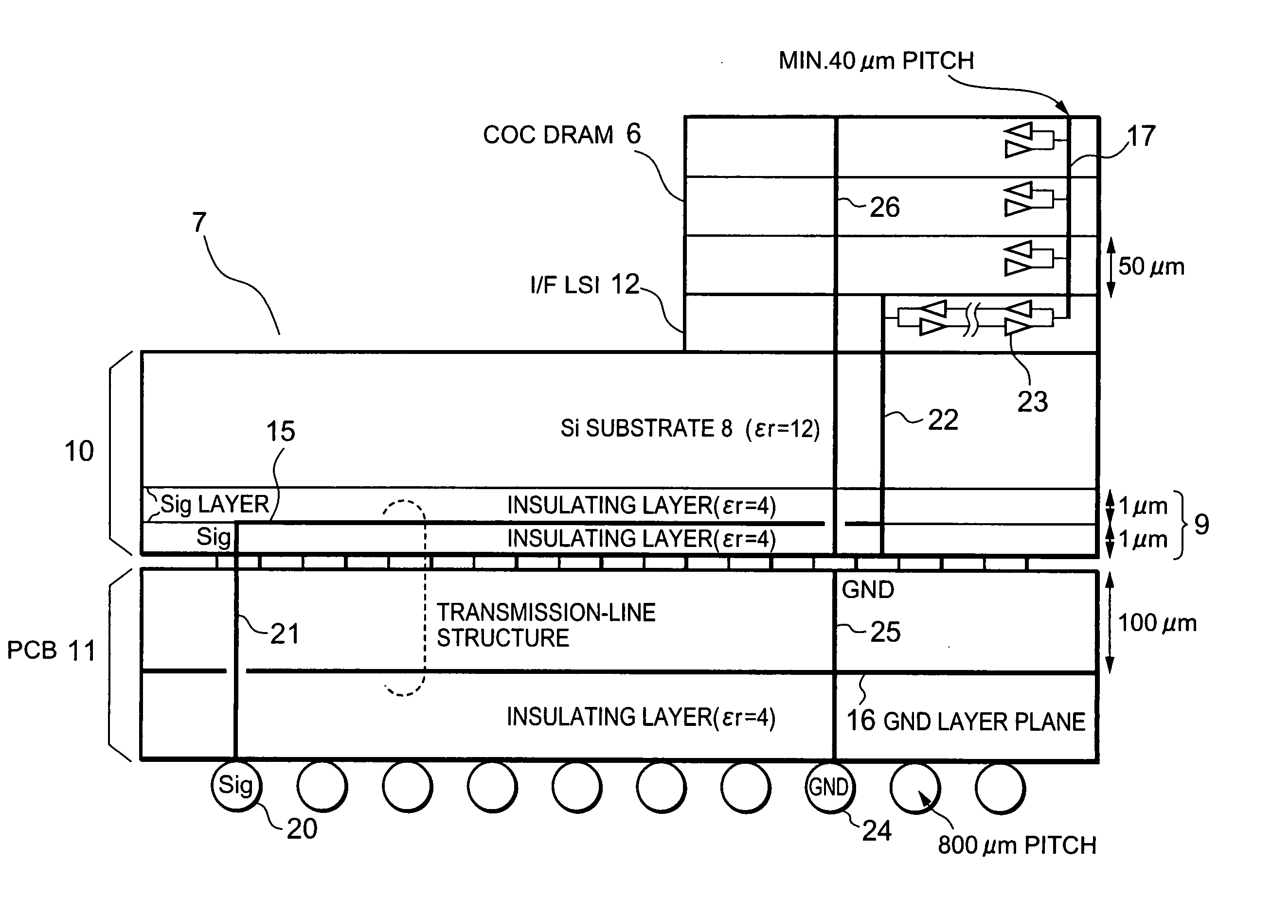
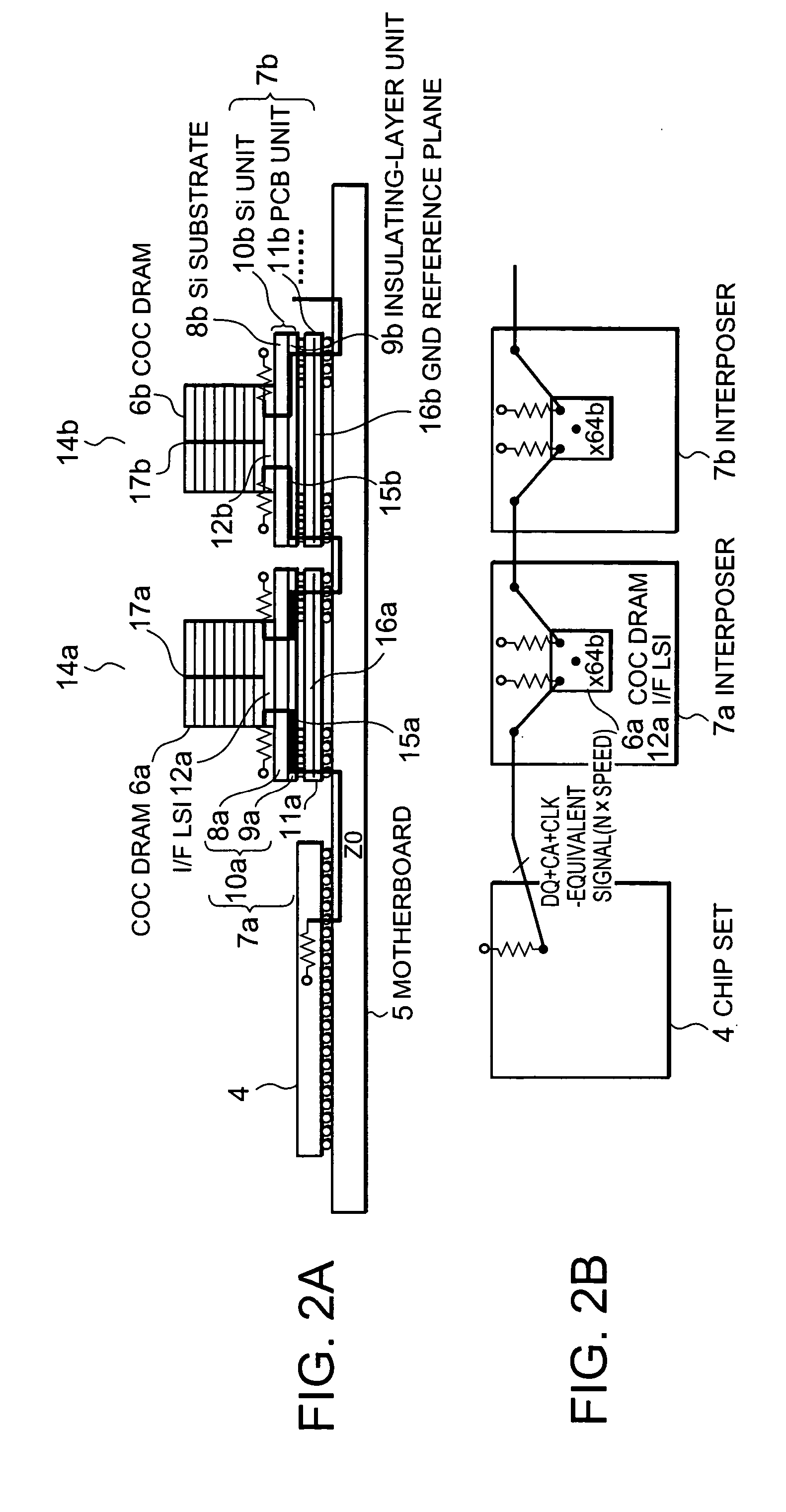
[0066]FIGS. 2A and 2B schematically show the configuration of a memory system (semiconductor integrated circuit (IC) device) according to the present invention, in which FIG. 2A is a longitudinal cross-sectional view and FIG. 2B is a plan view.

[0067] The memory system shown in FIGS. 2A and 2B includes a chip set 4 mounted on a motherboard 5 and a plurality of (two of them are shown here) stacked DRAMs 14a and 14b. Each of the stacked DRAMs 14a and 14b includes a chip on chip DRAM (COC DRAM) 6a (6b) including 8 to 16 stacked DRAM chips, an interface LSI (I / F LSI) 12a (12b) on which the COC DRAM 6a (6b) is stacked, and an interposer 7a (7b) which is disposed under the I / F LSI 12a (12b) and which includes a silicon (Si) unit 10a (10b) and a printed circuit board (PCB) 11a (11b).

[0068] The Si unit 10a (10b) of the interposer 7a (7b) includes a Si substrate 8a (8b) and an insulating-layer unit 9a (9b). The Si unit 10a (10b) and the PCB 11a (11b) of the interposer 7a (7b) are connected t...

second embodiment

[0134]FIG. 8 is a schematic view showing the configuration of a memory system according to the present invention. In FIG. 8, parts which are the same as those in FIGS. 2A and 2B are denoted by the same reference numerals.

[0135] The basic configuration of the memory system according to the second embodiment is the same as that in the first embodiment. The difference between these embodiments is that coaxial compact high-frequency connectors 80 are used instead of solder balls for connecting the PCB 11 and the motherboard 5. By using the connectors, the high-speed performance can be further enhanced.

[0136] Next, a method for placing the I / F LSI 12, which is common to the memory systems according to the first and second embodiments, will be explained with reference to FIGS. 9A and 9B.

[0137] As will be understood from FIGS. 9A and 9B, when the number of signals 85 (in this case, 1) input / output to / from the I / F LSI 12 through its lower surface is different from the number of signals 86...

third embodiment

[0147] Next, a memory system according to the present invention will be described with reference to FIGS. 11A and 11B. In FIGS. 11A and 11B, parts which are the same as those in FIGS. 2A and 2B are denoted by the same reference numerals.

[0148] The difference between the memory system shown in FIGS. 11A and 11B and that in FIGS. 2A and 2B is that each of stacked DRAMs 100 does not include the I / F LSI 12 and that a chip set 102 and the stacked DRAMs 100 are connected by a kind of point-to-point connection (one to plurality connection). That is, in the memory system according to the third embodiment, each of the stacked DRAMs 100 includes the COC DRAM 6 and the interposer 7, and a corresponding ball of all the stacked DRAM 100 is connected to each ball under the chip set 102. The chip set 102 and the COC DRAM 6 directly transmit / receive signals without using the I / F LSI 12.

[0149] The characteristic impedance of each signal line for connecting the chip set 102 and the stacked DRAM 100 ...


PUM


Abstract

A COC DRAM including a plurality of stacked DRAM chips is mounted on a motherboard by using an interposer. The interposer includes a Si unit and a PCB. The Si unit includes a Si substrate and an insulating-layer unit in which wiring is installed. The PCB includes a reference plane for the wiring in the Si unit. The wiring topology between a chip set and the COC DRAM is the same for every signal. Accordingly, a memory system enabling a high-speed operation, low power consumption, and large capacity is provided.

Description

[0001] This application claims priority to prior application JP 2003428888, the disclosure of which is incorporated herein by reference. BACKGROUND OF THE INVENTION [0002] 1. Field of the Invention [0003] The present invention relates to a semiconductor integrated circuit (IC) device. In particular, the present invention relates to a semiconductor IC device including a stacked dynamic random access memory (stacked DRAM) or a chip on chip DRAM (COC DRAM). [0004] 2. Description of the Related Art [0005]FIG. 1 shows an example of a memory system which is presently studied by Joint Electron Device Engineering Council (JEDEC). [0006] The memory system shown in FIG. 1 includes a chip set 4 mounted on a motherboard (not shown) and a plurality of (two of them are shown here) dual inline memory modules (DIMMs) 1a and 1b for transmitting / receiving signals to / from the chip set 4. A buffer 2a or 2b and a plurality of (8 in this case) DRAM chips 3a or 3b are mounted on each of the DIMMs 1a and 1...

Claims


Application Information

Patent Timeline
IPC IPC(8): G06F1/18H01L23/14G06F13/00G11C5/02G11C7/00G11C11/407H01L21/68H01L23/02H01L23/498H01L23/50H01L23/66H01L25/065H01L25/07H01L27/108H05K1/14
CPCG06F1/184G06F1/185H01L2924/13091G06F1/186G11C5/025H01L21/6835H01L23/49822H01L23/49833H01L23/50H01L23/66H01L2221/6834H01L2221/68368H01L2224/16H01L2924/01004H01L2924/0102H01L2924/15311H01L2924/19041H01L2924/30105H01L2924/3011H05K1/141H01L2924/01068H01L2924/00
Inventor NISHIO, YOJIFUNABA, SEIJI
Owner PS4 LUXCO SARL
Why Eureka
Try Eureka