Semiconductor device and method of manufacture thereof
A manufacturing method, semiconductor technology, applied in semiconductor/solid-state device manufacturing, semiconductor devices, semiconductor/solid-state device components, etc., can solve problems such as complex manufacturing process and high cost
- Summary
- Abstract
- Description
- Claims
- Application Information
AI Technical Summary
Problems solved by technology
Method used
Image

Examples
Embodiment approach 1
[0025] FIG. 1 is a cross-sectional view of a semiconductor device according to Embodiment 1 of the present invention. The semiconductor device 10 includes an insulating substrate 12 . The insulating substrate 12 is made of, for example, AlN, Al 2 o 3 , SiN, etc. are formed. Wiring patterns 14 a and 14 b are formed on the insulating substrate 12 . A relay terminal 14 c is also formed on the insulating substrate 12 . The relay terminal 14c is formed of the same material as the wiring patterns 14a and 14b such that one end is fixed to the insulating substrate 12 and the other end extends upward of the insulating substrate 12 .
[0026] A rear surface pattern 16 is formed on the rear surface of the insulating substrate 12 . The rear surface pattern 16 and the wiring patterns 14a and 14b are made of aluminum with a thickness of 1 to 5 mm. The semiconductor chip 20 is fixed to the wiring pattern 14b with solder 18 . The semiconductor chip 20 is formed of, for example, an IGBT...
Embodiment approach 2
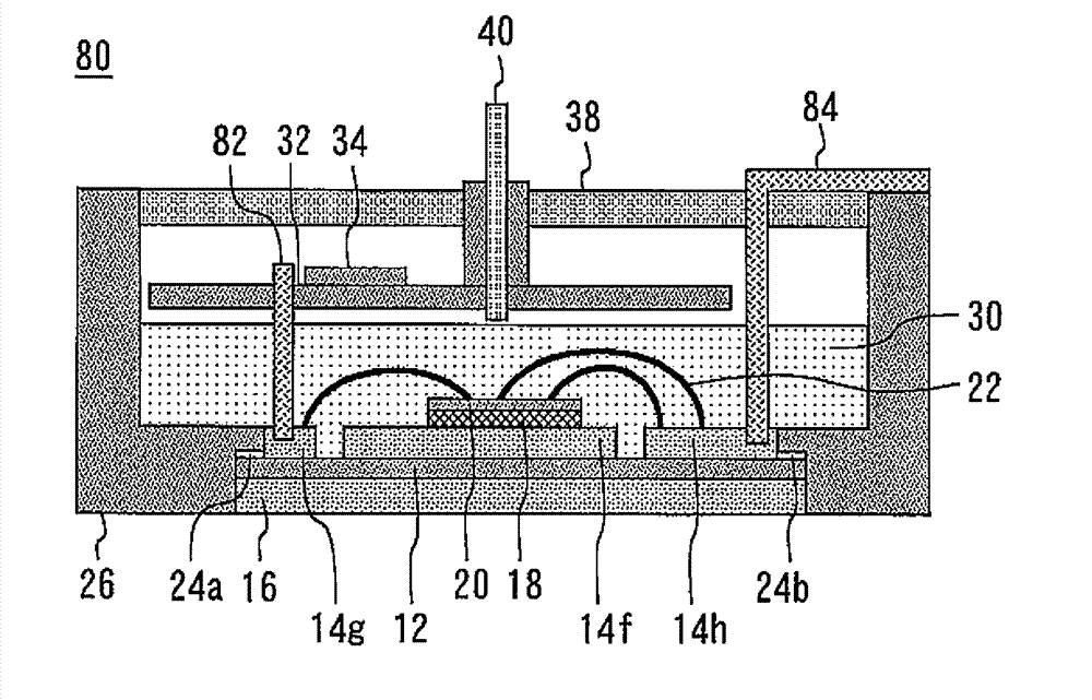
[0033] The semiconductor device and its manufacturing method according to Embodiment 2 of the present invention have many points in common with Embodiment 1, and therefore, differences from Embodiment 1 will be mainly described. 3 is a cross-sectional view of a semiconductor device according to Embodiment 2 of the present invention. The semiconductor device 50 includes a power terminal 14d. The power terminal 14 d is formed such that one end is fixed to the insulating substrate 12 and the other end extends upward of the insulating substrate 12 . The power terminal 14d is formed of aluminum which is the same material as the wiring pattern 14b. Therefore, all of the power terminal 14d, the wiring pattern 14b, the relay terminal 14c, and the rear surface pattern 16 are formed of aluminum. Furthermore, the power terminal 14d is electrically connected to the semiconductor chip 20 by the lead wire 22 .
[0034] Next, a method of manufacturing a semiconductor device according to E...
Embodiment approach 3
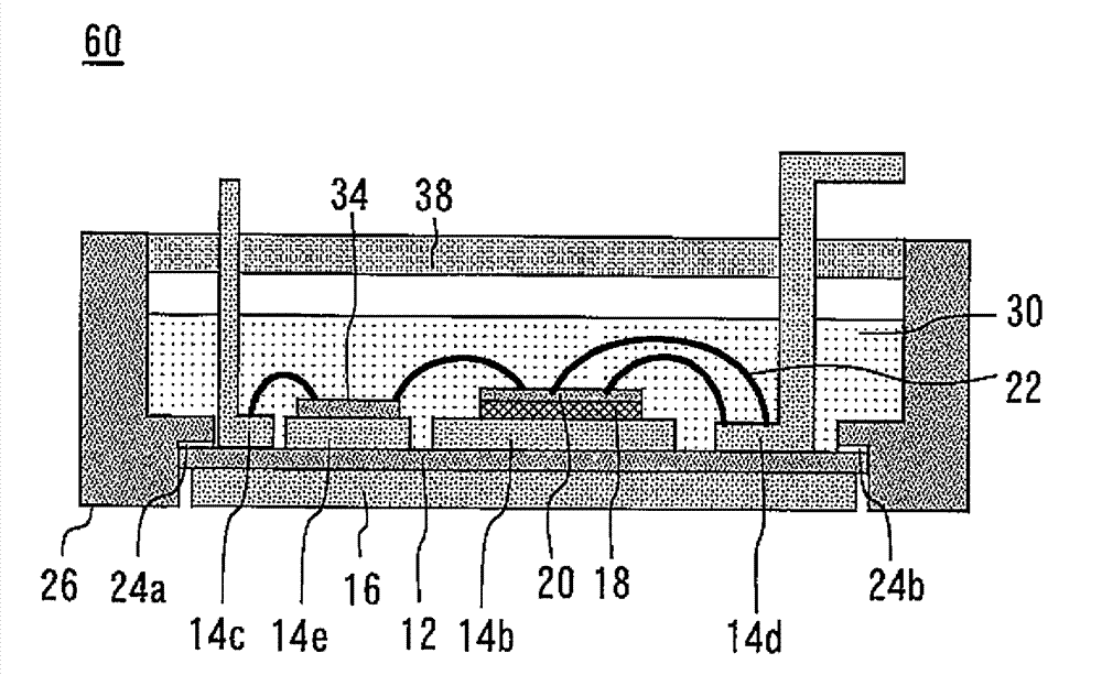
[0037] The semiconductor device and its manufacturing method according to Embodiment 3 of the present invention have many points in common with Embodiment 1, and therefore, differences from Embodiment 1 will be mainly described. 5 is a cross-sectional view of a semiconductor device according to Embodiment 3 of the present invention. The semiconductor device 60 includes a control circuit wiring pattern 14 e formed on the insulating substrate 12 . The control circuit wiring pattern 14e is formed of aluminum which is the same material as the wiring pattern 14b. Therefore, the control circuit wiring pattern 14e, the power terminal 14d, the wiring pattern 14b, the relay terminal 14c, and the rear surface pattern 16 are all formed of aluminum. The control circuit 34 is fixed to the control circuit wiring pattern 14e. The control circuit 34 is connected to the semiconductor chip 20 and the relay terminal 14 c by the lead wire 22 . Also, the control circuit 34 is sealed with silico...
PUM
 Abstract
Description
Claims
Application Information
 - R&D
- Intellectual Property
- Life Sciences
- Materials
- Tech Scout
- Unparalleled Data Quality
- Higher Quality Content
- 60% Fewer Hallucinations
Browse by: Latest US Patents, China's latest patents, Technical Efficacy Thesaurus, Application Domain, Technology Topic, Popular Technical Reports.
© 2025 PatSnap. All rights reserved.Legal|Privacy policy|Modern Slavery Act Transparency Statement|Sitemap|About US| Contact US: help@patsnap.com