Liquid crystal display device
A liquid crystal display device and liquid crystal panel technology, which is applied to lighting devices, lighting device parts, optics, etc., can solve the problems of light leakage at the edge of the liquid crystal display, the light cannot be absorbed, and the black edge of printing cannot be realized, and the side edge can be improved. Light leakage problem, the effect of reducing light
- Summary
- Abstract
- Description
- Claims
- Application Information
AI Technical Summary
Problems solved by technology
Method used
Image
Examples
Embodiment 1
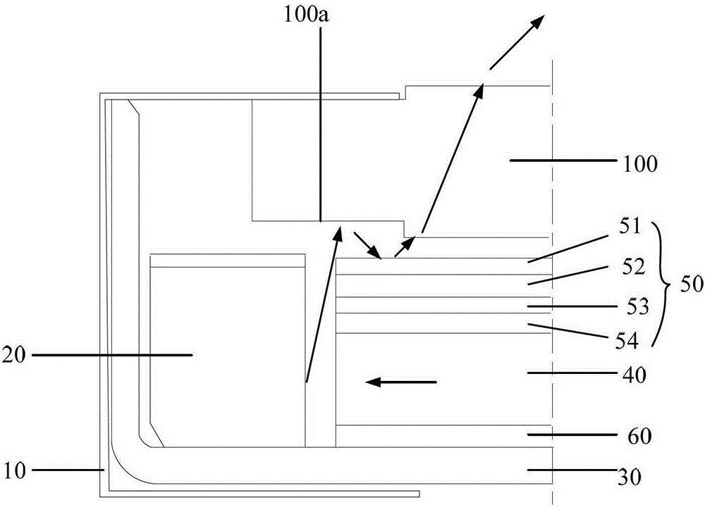
[0044] Figure 4 Shown is a schematic structural diagram of the liquid crystal display device in the first embodiment provided by the present invention. In the liquid crystal display device provided in this embodiment, a light absorbing layer is formed on the bottom reflection sheet located on the side of the light guide plate close to the back plate to improve the phenomenon of light leakage at the side of the liquid crystal display device.
[0045] Specifically, such as Figure 4 As shown, the liquid crystal display device provided in this embodiment includes:
[0046] LCD panel 100
[0047] A back plate 30 arranged opposite to the liquid crystal panel 100;
[0048] The bottom reflector 60, the light guide plate 40 and the optical film 50 are arranged between the back plate 30 and the liquid crystal panel 100, wherein the bottom reflector 60, the light guide plate 40 and the optical film 50 approach the liquid crystal from the side close to the back plate 30 One side of the panel 1...
Embodiment 2
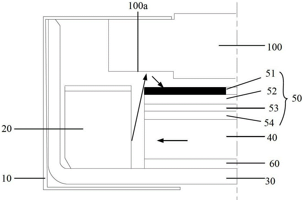
[0057] Figure 5 Shown is a schematic structural diagram of the second embodiment provided by the present invention. Such as Figure 5 As shown, in this embodiment, the light-absorbing layer 200 is also disposed on the bottom reflector 60. Compared with the first embodiment provided by the present invention, the difference is only that the end of the plastic frame 20 close to the light guide plate 40 is A cavity is formed at a position corresponding to the light guide plate 40 (ie, the second inner end surface 202), and the outer end surface of the light guide plate 40 close to the plastic frame 20 extends into the cavity, so that the light guide plate 40 is far from the back plate 30 There will be a partial overlap between the light emitting surface and the plastic frame 20, and the end of the bottom reflective sheet 60 close to the plastic frame 20 also extends into the cavity. At this time, the light absorbing layer 200 is formed on the bottom reflective sheet 60 near the pla...
Embodiment 3
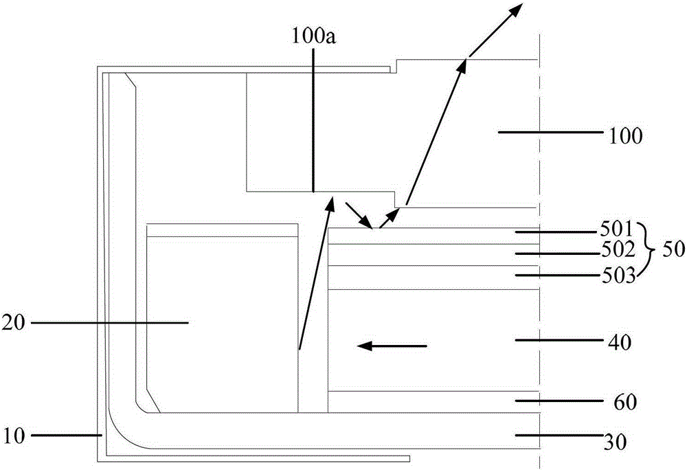
[0059] Image 6 Shown is a schematic structural diagram of a liquid crystal display device in a third embodiment provided by the present invention. In the liquid crystal display device provided in this embodiment, the light absorbing layer 200 is formed on the lower diffusion sheet of the optical film 50 on the side of the light guide plate 40 away from the back plate 30 to improve the side light leakage of the liquid crystal display device.
[0060] Specifically, such as Image 6 As shown, the liquid crystal display device provided in this embodiment includes:
[0061] LCD panel 100;
[0062] A back plate 30 arranged opposite to the liquid crystal panel 100;
[0063] The bottom reflector 60, the light guide plate 40 and the optical film 50 are arranged between the back plate 30 and the liquid crystal panel 100, wherein the bottom reflector 60, the light guide plate 40 and the optical film 50 approach the liquid crystal from the side close to the back plate 30 One side of the panel 1...
PUM
 Abstract
Description
Claims
Application Information


