Method and system for adaptively adjusting working voltage of chips

A technology of self-adaptive adjustment and working voltage, applied in information storage, static memory, digital memory information, etc., can solve the problems of increasing chip production cost and chip power consumption, and achieve the effect of reducing production test cost and controlling power consumption

Inactive Publication Date: 2013-04-24
GUANGDONG NUFRONT COMP SYST CHIP
View PDF4 Cites 9 Cited by
  • Summary
  • Abstract
  • Description
  • Claims
  • Application Information

AI Technical Summary

Problems solved by technology

[0006] Obviously, the first method will cause excessive waste of power consumption for the 0.9V chip, and the second method will increase the production cost of the chip

Method used


Image

  • Method and system for adaptively adjusting working voltage of chips
  • Method and system for adaptively adjusting working voltage of chips
  • Method and system for adaptively adjusting working voltage of chips

Examples


Embodiment 1

[0074] The leakage current of the chip (leakage) has a certain corresponding relationship with the working voltage of the chip

[0075] The corresponding relationship between the leakage current of the chip and the working voltage is obtained through a large number of experiments on the test machine. Specifically, a curve of the leakage current and the working voltage can be fitted through the experimental data.

[0076] It can be seen that a chip with a small leakage current requires a large operating voltage, and a chip with a large leakage current requires a smaller operating voltage. Based on this, the present invention proposes a method for adaptively adjusting the operating voltage of the chip, which is specifically divided into two stages:

[0077] Ⅰ. Chip testing stage

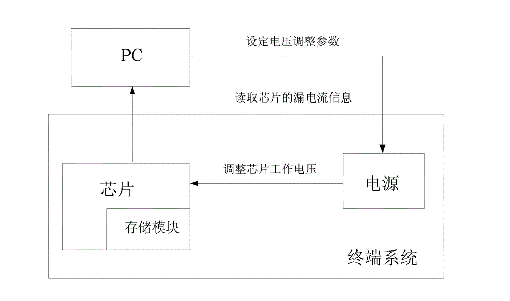
[0078] Figure 4 This is a schematic diagram of the principle of obtaining the leakage current value in this embodiment. Reference Figure 4 , When the chip is tested for ATE, the leakage current of the chip i...

Embodiment 2

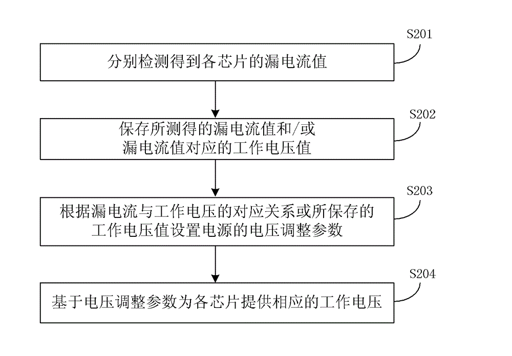
[0084] Such as Image 6 As shown, another method for adaptively adjusting the operating voltage of a chip provided in this embodiment includes the following steps:

[0085] S601: Scan all possible working voltages to determine the lowest working voltage of each chip;

[0086] Scan to get a set of voltage values ​​(range) to determine the lowest operating voltage of each chip.

[0087] There are also various methods for scanning the lowest voltage of the chip, mainly including the following two:

[0088] 1) Put multiple chips on the actual system board, run a special test program, gradually adjust the operating voltage of the chip, and observe the operating status of the chip to determine the final operating voltage.

[0089] 2) Put the chip on the automatic test platform, drive a special test excitation by ATE, and determine the working voltage by shamoo.

[0090] S602: Save the minimum operating voltage value of each chip;

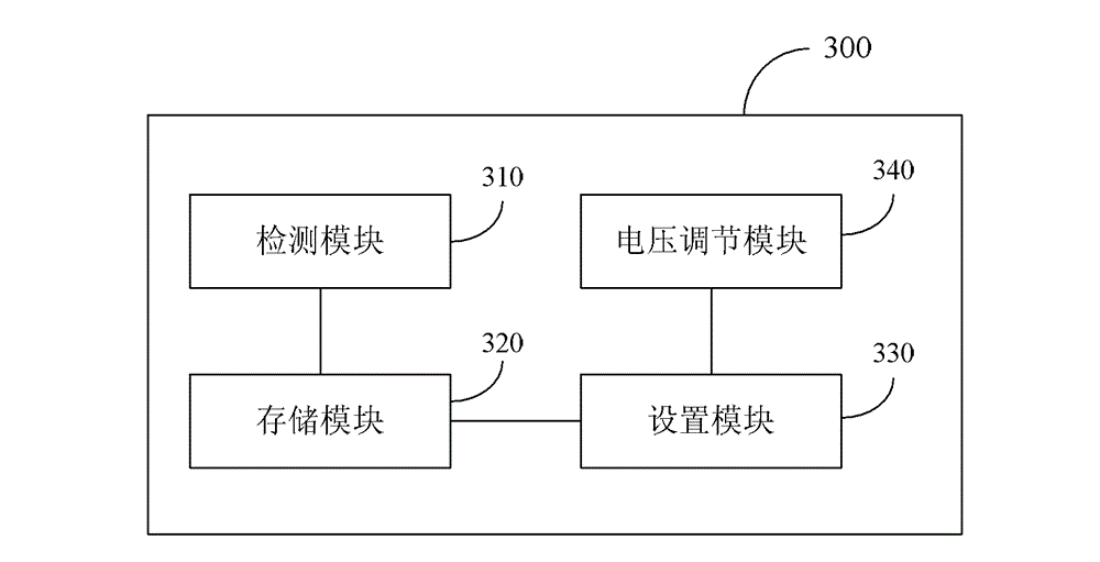
[0091] Save it in storage media, such as eFuse, electrically er...


PUM


Abstract

The invention discloses a method for adaptively adjusting working voltage of chips. The method comprises the following steps of: respectively detecting to obtain a leakage current value of each chip; saving the obtained leakage current value and/or a working voltage value corresponding to the leakage current value; setting a voltage adjustment parameter of a power supply according to the corresponding relation between the leakage current value and the working voltage or a saved working voltage value; and providing the corresponding working voltage for each chip based on the voltage adjustment parameter. The invention also provides a system for adaptively adjusting working voltage of the chips. The lowest working voltage of each chip is determined according to the relation between the leakage current value and the working voltage, and the working voltage of the chip is adjusted to the lowest working voltage after the chip is started, so that the working voltage of the chip can be determined according to the physical property of the chip based on the condition of different working voltages caused by the chip difference brought by a chip manufacturing procedure, therefore, the power consumption of the chip is effectively controlled, and the cost of a production test is reduced.

Description

technical field [0001] The invention relates to the technical field of integrated circuit manufacturing and application, in particular to a method and system for adaptively adjusting chip operating voltage. Background technique [0002] With the continuous improvement of the chip manufacturing process, it gradually develops into a finer process, for example, from 80 nanometers to 40 nanometers, or even 28 nanometers, especially after the process reaches 40 nanometers, as a semiconductor element "grain" or "chip" The difference between the substrate wafer (wafer) and the wafer, and between chips is getting bigger and bigger. Reflected in the actual system, the working voltage required by different chips is very different, and some may be able to It can work on 0.9V, but some chips really need 0.95V to work normally. [0003] In order to solve this problem, the following methods are usually adopted in the prior art: [0004] 1) Provide the working voltage of the chip as a wh...

Claims


Application Information

Patent Timeline
Patent Type & Authority Applications(China)
IPC IPC(8): G11C7/24
Inventor 季云建丁杰鲍东山
Owner GUANGDONG NUFRONT COMP SYST CHIP
Why Eureka
Try Eureka