Wafer surface treatment device

A surface treatment device, wafer technology, applied in electrical components, semiconductor/solid-state device manufacturing, circuits, etc., can solve the problems of the wafer cannot be rotated, the wafer is damaged, difficult to clean horizontally, electroplating or etching, etc., to reduce Risk of damage to wafer, uniform etching, ease of use effect

Active Publication Date: 2013-04-24
SHANGHAI SINYANG SEMICON MATERIALS
View PDF6 Cites 9 Cited by
  • Summary
  • Abstract
  • Description
  • Claims
  • Application Information

AI Technical Summary

Problems solved by technology

Although this device can process the surface of the wafer to a certain extent, the wafer cannot be rotated and cannot guarantee uniform surface treatment.
This surface device is difficult to achieve horizontal cleaning, electroplating or etching, that is, the wafer is placed horizontally above the cleaning solution, plating solution or etching solution, and the cleaning solution, plating solution or etching solution flows from bottom to top until it contacts the wafer. Clean the wafer surface
Another disadvantage of cleaning is that the spray water is directly sprayed on the wafer, and the wafer is easily damaged if the water pressure is too high.

Method used


Image

  • Wafer surface treatment device
  • Wafer surface treatment device
  • Wafer surface treatment device

Examples


Embodiment 1

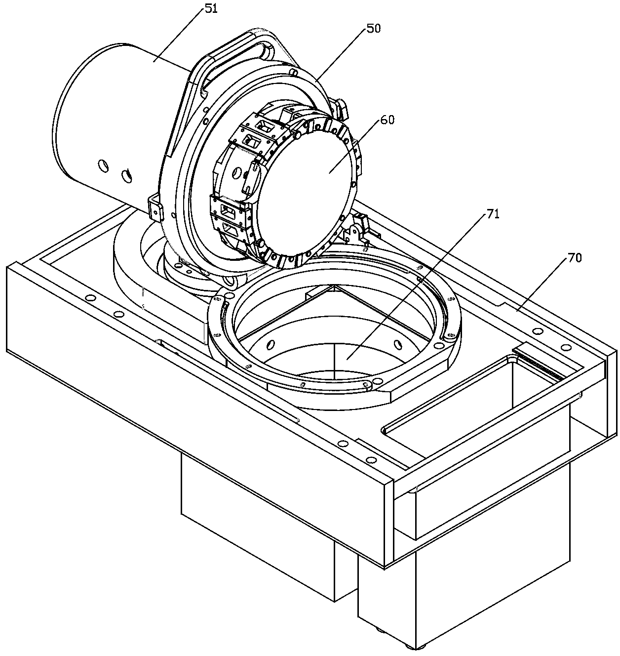
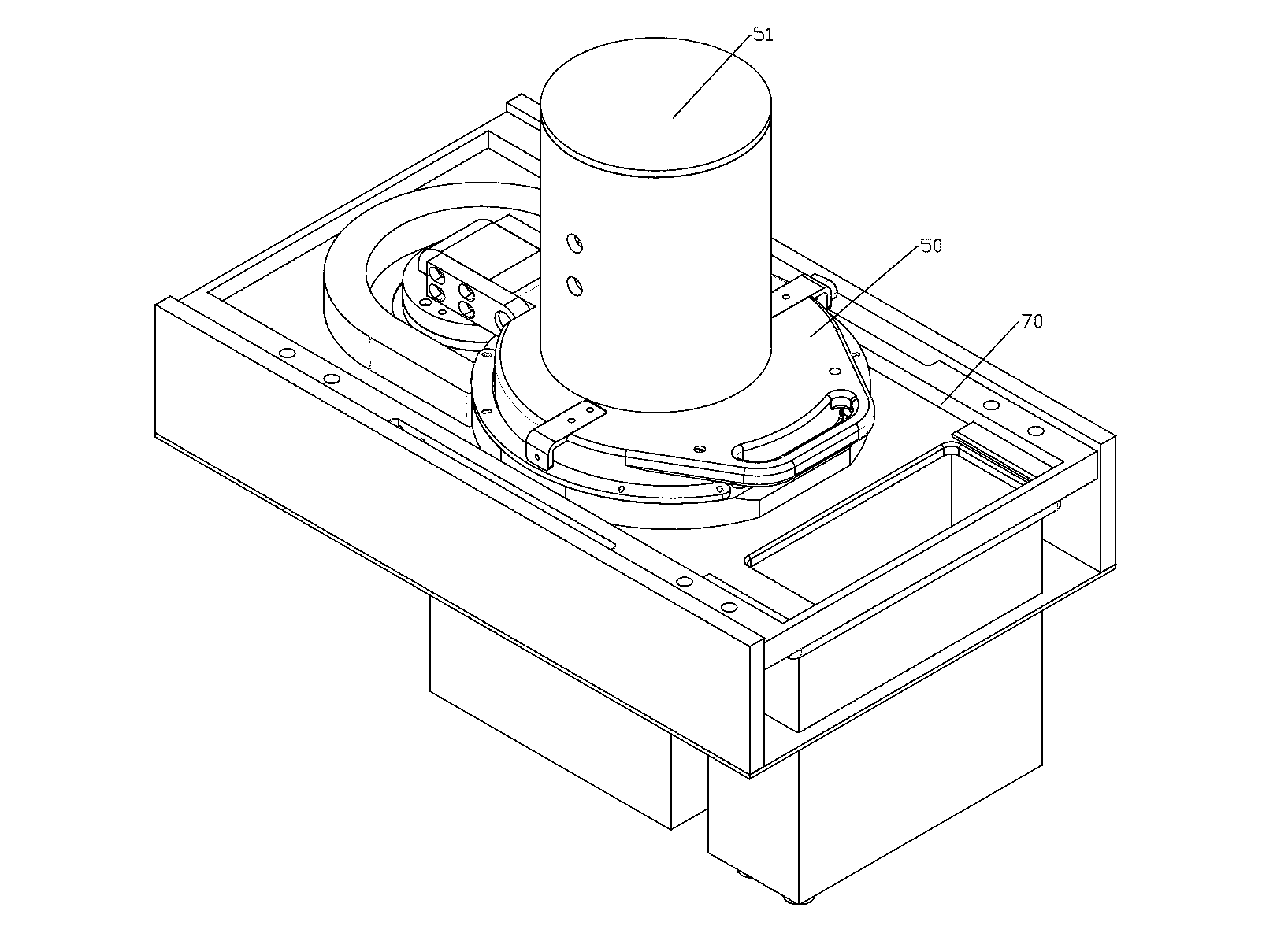
[0040] Such as figure 1 , figure 2 As shown, the wafer surface processing device includes a wafer clamping and rotating device and a tank 70 . The tank body 70 is provided with a tank cavity 71 . The tank cover 50 is hinged on the tank body 70 and is reversibly installed. After the wafer 60 is fixed, turn over the slot cover 50 to make it as Figure 6 As shown in the sealed tank cavity 71 , cleaning water enters from the lower end of the tank body 70 and flows upward to the position where it contacts the wafer 60 to clean the wafer 60 . During the cleaning process, the wafer clamping and rotating device drives the wafer 60 to rotate.

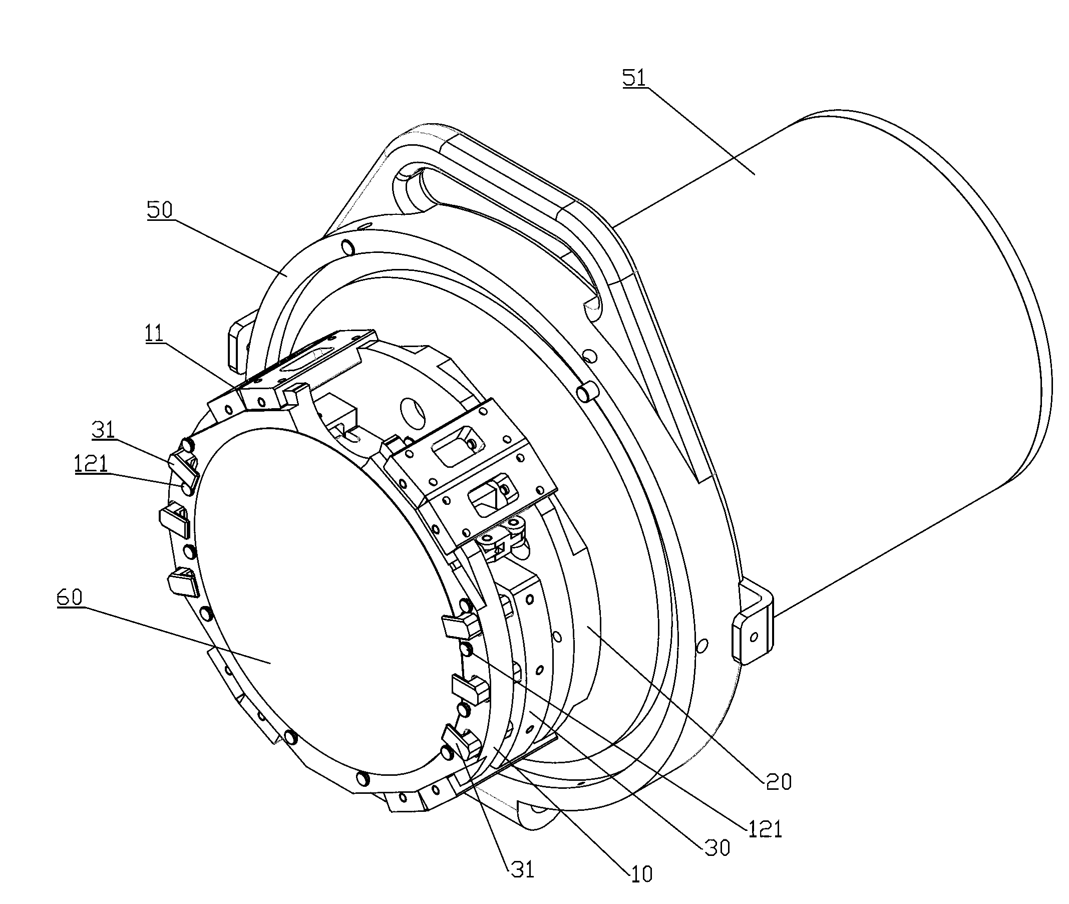
[0041] Such as image 3 , Figure 4 , Figure 5 and Figure 6 As shown, the wafer holding and rotating device includes a slot cover 50 . A casing 51 is mounted on the slot cover 50 . The casing 51 has a cavity 52 . A cylindrical bracket 521 and a motor 54 are disposed in the cavity 52 . The cylinder 53 includes a housing 531 , a pis...

Embodiment 2

[0046] The difference between this embodiment and Implementation 1 is that, as Figure 7 As shown, no sleeve 55 is provided. The housing 531 of the air cylinder is rotatably mounted on the tank cover 50 and connected to the upper base plate 30 after passing through the tank cover 50 . The piston plate 56 is movably disposed in the casing 531 . An O-ring 58 is disposed between the housing 531 and the slot cover 50 . The rest of the structure is the same as in Implementation 1.

[0047] The compression spring 57 in Embodiment 1 and Embodiment 2 can also be arranged between the support plate 30 and the lower base plate 10 , with one end abutting against the support plate 30 and the other end abutting against the lower base plate 10 . Of course, the compression spring 57 can also be replaced by a tension spring, the tension spring is arranged between the upper base plate 20 and the support plate 30 , and its two ends are respectively connected with the upper base plate 20 and t...


PUM


Abstract

The invention discloses a wafer surface treatment device which is characterized by comprising a wafer clamping rotating device and a groove body. The groove body is provided with a groove cavity. The wafer clamping rotating device is hinged at the upper end of the groove body and arranged in a turning mode. The wafer clamping rotating device is composed of a lower base plate and a clamping clip, and the lower base plate is used for fixing a wafer and arranged in a rotating mode. The clamping clip consists of a hook body which extends toward the center of the base plate. The hook body is arranged below the lower base plate. The hook body which is driven to conduct motion toward the lower base plate and conduct reciprocating motion away from the lower base plate is arranged. The wafer surface treatment device not only fixes the wafer, but also drives the wafer to rotate. Even treatment on the surface of the wafer can be ensured after cleaning, galvanizing or etching. When cleaning is conducted, cleanout liquid does not need spraying the wafer, and risk of damage of the wafer can be reduced. When galvanizing or the etching is conducted, not only can each part of a galvanized or etched wafer be ensured, but also the galvanizing or the etching can be ensured. Meanwhile, the wafer surface treatment device is convenient to use.

Description

technical field [0001] The invention relates to a wafer surface treatment device. Background technique [0002] During the wafer production process, its surface needs to be treated, such as cleaning, plating or etching. A commonly used surface cleaning method is to fix the wafer in a cleaning tank, and spray the cleaning solution to the wafer. The spraying device of the cleaning fluid is in constant motion to thoroughly clean the wafer. Electroplating or etching is the same method. Although this device can process the surface of the wafer to a certain extent, the wafer cannot be rotated and cannot ensure uniform surface treatment. This surface device is difficult to achieve horizontal cleaning, electroplating or etching, that is, the wafer is placed horizontally above the cleaning solution, plating solution or etching solution, and the cleaning solution, plating solution or etching solution flows from bottom to top until it contacts the wafer. Clean the wafer surface. A...

Claims


Application Information

Patent Timeline
Patent Type & Authority Applications(China)
IPC IPC(8): H01L21/67H01L21/687
Inventor 吕海波王振荣刘红兵
Owner SHANGHAI SINYANG SEMICON MATERIALS
Why Eureka
Try Eureka