A package welding method and device

A technology for welding devices and packaging devices, applied in welding equipment, metal processing equipment, manufacturing tools, etc., can solve the problems of large temperature gradient, difficulty in finding suitable solder, low efficiency, etc., and achieve the effect of improving welding efficiency

Active Publication Date: 2015-09-02
YANTAI RAYTRON TECH
View PDF10 Cites 0 Cited by
  • Summary
  • Abstract
  • Description
  • Claims
  • Application Information

AI Technical Summary

Problems solved by technology

[0005] The technical problem to be solved by the present invention is to solve the shortcomings of large temperature gradient caused by a single heating mode in the prior art, difficulty in finding suitable solder and low efficiency caused by two times of welding, and provide a packaging and welding device and method with high production efficiency

Method used


Image

  • A package welding method and device
  • A package welding method and device
  • A package welding method and device

Examples


Embodiment Construction

[0043] The principles and features of the present invention are described below in conjunction with the accompanying drawings, and the examples given are only used to explain the present invention, and are not intended to limit the scope of the present invention.

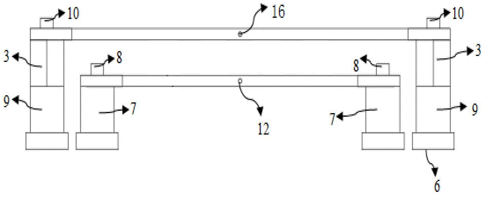
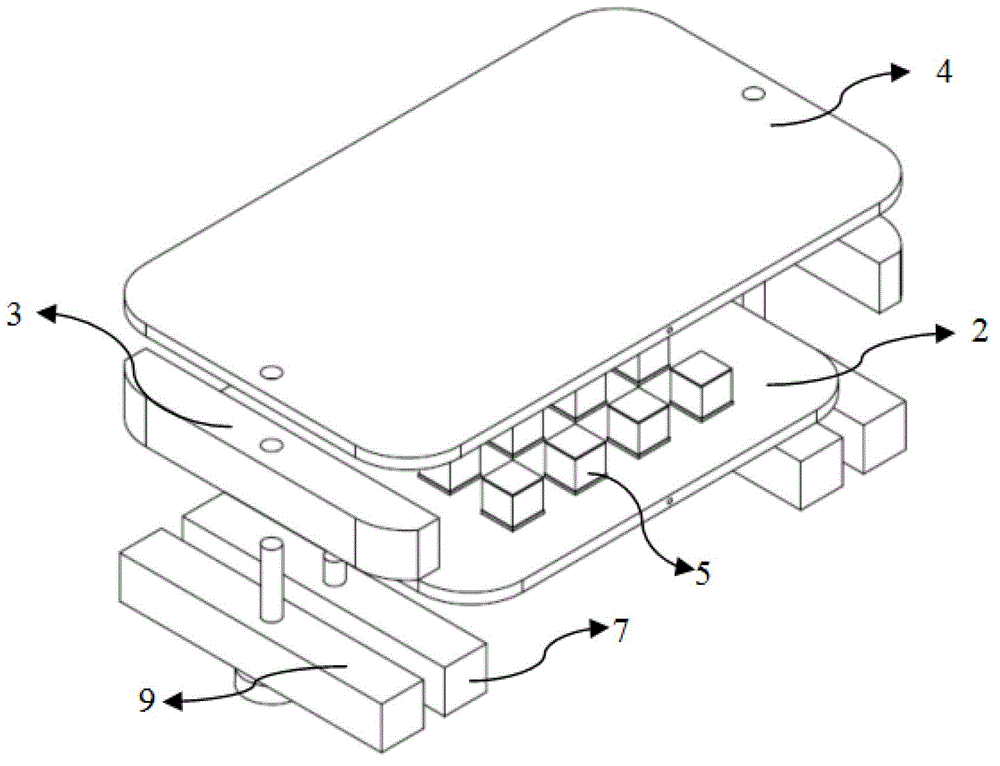
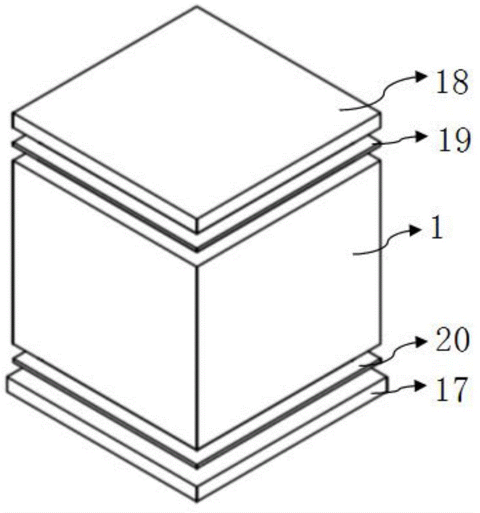
[0044] The present invention adopts the mode that two pairs of electrodes respectively control the upper and lower heating plates, and simultaneously treats the substrate 17 and the cover plate 18 of the packaged device 5 (such as image 3 ) to heat the cover plate solder 19 and the base plate solder 20 to complete the welding of the cover plate 18 , the base plate 17 and the shell 1 . image 3It is a separation diagram of the main components of the present invention, mainly including the metal electrode 9 of the upper heating plate, the metal electrode 7 of the lower heating plate, the lower heating plate 2, the conductive block 3, the upper heating plate 4 and the device 5 to be packaged.

[0045] Metal electrodes...


PUM


Abstract

The invention relates to the field of semiconductor package, in particular to a package welding method and a package welding device. The technical scheme for solving the technical problem is that the package welding method is characterized by comprising the following steps of: 1, placing a device to be packaged on a lower heating plate of a welding furnace; 2, fixing an upper heating plate through a metal electrode and a conductive block to place the upper heating plate at the upper end of the device to be packaged; and 3, controlling temperatures of the upper heating plate and the lower heating plate to finish welding of the device to be packaged. The package welding method has the beneficial effects that the device, of which a plurality of components are required to be welded, is simultaneously heated from the bottom and the top together in a mode of heating through the upper heating plate and the lower heating plate together, the problems of large temperature difference of each welding point caused by heat resistance of each component of the device to be packaged and influence on welding efficiency are solved, and the welding efficiency is increased.

Description

technical field [0001] The invention relates to the field of semiconductor packaging, in particular to a packaging welding method and device. Background technique [0002] The packaging process of semiconductor products involves chip welding, cover plate welding and window welding. The welding method is generally in a nitrogen protection environment or a vacuum environment, heating and melting solder or solder paste to assemble the chip and the substrate, the cover plate and the shell or other components. Usually more than one part of a product needs to be welded, such as a MEMS device package, using solder to weld the cover, substrate and shell to form a hermetic packaged device. [0003] The package of the device has two welding surfaces, that is, the welding of the cover plate and the shell and the welding of the shell and the substrate. At present, there are two main methods for welding: 1) Using the same solder, put all components together into the heating furnace The...

Claims


Application Information

Patent Timeline
Patent Type & Authority Patents(China)
IPC IPC(8): B23K1/008
Inventor 陈文祥熊笔锋
Owner YANTAI RAYTRON TECH
Why Eureka
Try Eureka