Photonic crystal, color film substrate, display panel and display device
A photonic crystal and display panel technology, applied in optics, filters, optical components, etc., can solve the problem of low transmittance of display panels, and achieve the effect of improving transmittance and solving low transmittance.
- Summary
- Abstract
- Description
- Claims
- Application Information
AI Technical Summary
Problems solved by technology
Method used
Image

Examples
Embodiment 1
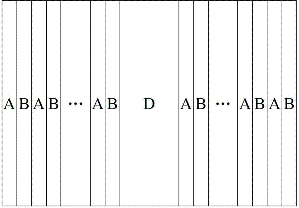
[0026] Such as figure 1 As shown, in the photonic crystal provided by the embodiment of the present invention, the forbidden band of the photonic crystal includes the visible light band, and the photonic crystal is provided with a defect layer. The wavelength range of the visible light band is 400-780nm. In this embodiment, the forbidden band can be set slightly wider than the visible light band. For example, the forbidden band can be set to 350-800nm or a wider range.
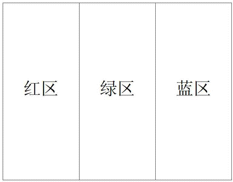
[0027] The photonic crystal at least includes a red zone, a green zone and a blue zone, the photonic crystal with a defective layer corresponding to the red zone is used to transmit red light, and the photonic crystal with a defective layer corresponding to the green zone is used to transmit green light, The photonic crystal with defect layer corresponding to the blue region is used to transmit blue light.
[0028] Further, the photonic crystal includes a red zone, a green zone, a blue zone and a yellow zon...
Embodiment 2
[0033] The embodiment of the present invention also provides a color filter substrate, including the photonic crystal film formed by the photonic crystal described in the first embodiment;
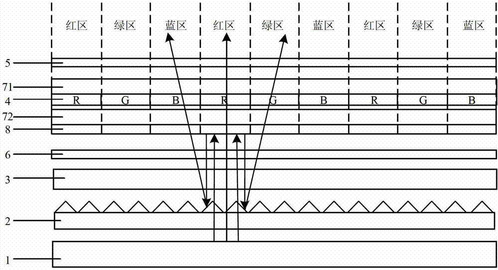
[0034] The photonic crystal film is located under the color film of the color film substrate, the color film substrate at least includes a red color film, a green color film and a blue color film, and the red area, green area, and blue area of the photonic crystal film are respectively connected to the The positions of red color film, green color film and blue color film are corresponding.
[0035] When the photonic crystal includes a red area, a green area, a blue area and a yellow area, the color film substrate includes a red color film, a green color film, a blue color film and a yellow color film.
[0036] The color filter substrate in this embodiment is provided with a photonic crystal film, and when applied to a display device, the light transmittance of the display device can be i...
Embodiment 3
[0038] An embodiment of the present invention provides a display panel, including the color filter substrate described in the second embodiment.
[0039] The embodiment of the present invention also provides another display panel, including the photonic crystal film formed by the photonic crystal described in the first embodiment;
[0040] The display panel also includes an upper polarizer and a lower polarizer, and the photonic crystal film is arranged on the lower polarizer. The photonic crystal film can be arranged above or below the lower polarizer.
[0041] The display panel also includes a color film substrate, the color film substrate at least includes a red color film, a green color film and a blue color film, and the red area and the green area of the photonic crystal film arranged on the lower polarizer are , and the blue area correspond to the positions of the red color film, the green color film, and the blue color film respectively. In the embodiment of the pr...
PUM
| Property | Measurement | Unit |
|---|---|---|
| Wavelength range | aaaaa | aaaaa |
Abstract
Description
Claims
Application Information
 - Generate Ideas
- Intellectual Property
- Life Sciences
- Materials
- Tech Scout
- Unparalleled Data Quality
- Higher Quality Content
- 60% Fewer Hallucinations
Browse by: Latest US Patents, China's latest patents, Technical Efficacy Thesaurus, Application Domain, Technology Topic, Popular Technical Reports.
© 2025 PatSnap. All rights reserved.Legal|Privacy policy|Modern Slavery Act Transparency Statement|Sitemap|About US| Contact US: help@patsnap.com