Touch control display panel
A technology for touch display panels and touch components, which is applied in the fields of instruments, electrical digital data processing, and data processing input/output processes, etc. The touch elements are made on the same substrate, etc., to achieve the effect of thinning the overall thickness
- Summary
- Abstract
- Description
- Claims
- Application Information
AI Technical Summary
Problems solved by technology
Method used
Image
Examples
no. 1 example
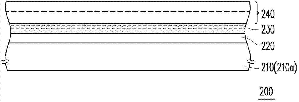
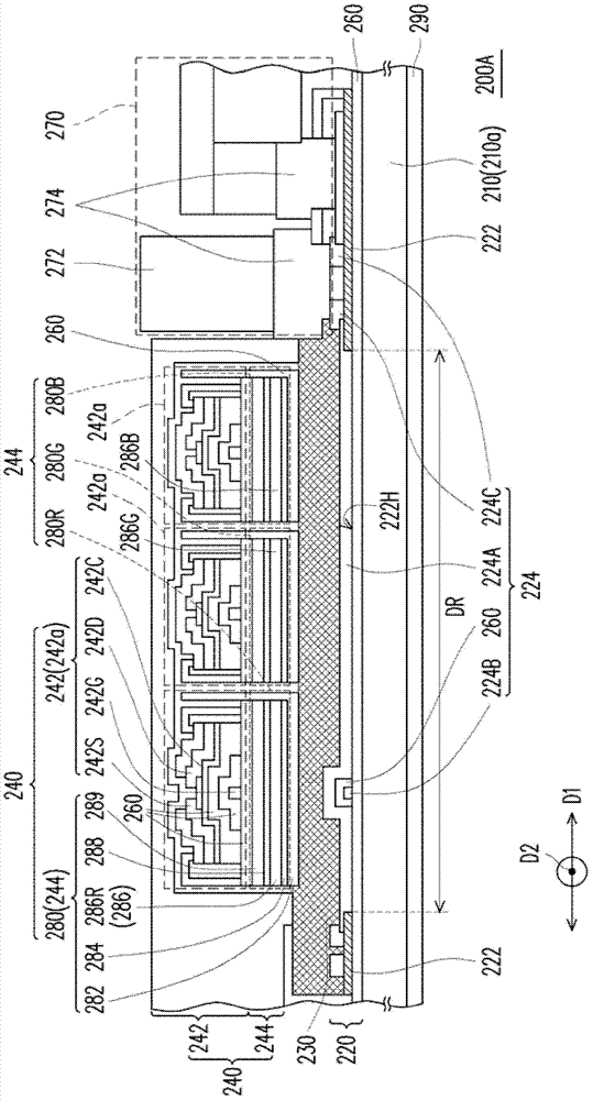
[0063] figure 2 It is a schematic cross-sectional structure diagram of a touch display panel in the first embodiment of the present invention, which is the aforementioned Figure 1A A schematic diagram of a specific structure. Please refer to figure 2 , the touch display panel 200A includes a transparent cover plate 210a, a touch element layer 220, an isolation layer 230, and a display element layer 240. In this embodiment, the touch display panel 200A and the display element layer 240 use the same transparent cover plate 210a As the carrier substrate, it simultaneously carries the laminated structure of the touch element layer 220 , the isolation layer 230 and the display element layer 240 .
[0064] like figure 2As shown, the touch element layer 220 includes a decoration layer 222 and a touch element array 224 . The decoration layer 222 and the touch element array 224 are located on the transparent cover 210a. The decoration layer 222 exposes an opening 222H on the tra...
no. 2 example
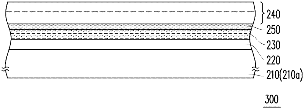
[0079] image 3 It is a schematic cross-sectional structure diagram of a touch display panel in the second embodiment of the present invention, and it is the aforementioned Figure 1B A schematic diagram of the specific structure. Please refer to image 3 , the touch display panel 300A and the aforementioned figure 2 The structure of the touch display panel 200A shown is similar, but in the touch display panel 300A of this embodiment, a shielding electrode layer 250 is also provided between the isolation layer 230 and the display element layer 240, thereby further avoiding touch The signal of the control element layer 220 and the signal of the display element layer 240 interfere with each other, which helps to improve the overall quality of the touch display panel 300A. Other components are the same as those in the first embodiment, please refer to the foregoing description, and the same components are represented by the same symbols.
no. 3 example
[0081] Figure 4 It is a schematic cross-sectional structure diagram of a touch display panel in the third embodiment of the present invention, and it is the aforementioned Figure 1B Another specific schematic diagram of the structure. Please refer to Figure 4 , the touch display panel 300B and the aforementioned image 3 The structure of the touch display panel 300A is shown, but the difference is that in the touch display panel 300B of this embodiment, the positions of the active element array 242 and the organic electroluminescent pixel array 244 are reversed, and the organic electroluminescent pixel array 244 The light emitted by 280 is also directed towards the transparent cover 210a. Other components are the same as those in the first embodiment, please refer to the foregoing description, and the same components are represented by the same symbols.
[0082] To sum up, in the touch display panel of the present invention, the isolation layer with a highly cross-linke...
PUM
 Abstract
Description
Claims
Application Information
 - R&D
- Intellectual Property
- Life Sciences
- Materials
- Tech Scout
- Unparalleled Data Quality
- Higher Quality Content
- 60% Fewer Hallucinations
Browse by: Latest US Patents, China's latest patents, Technical Efficacy Thesaurus, Application Domain, Technology Topic, Popular Technical Reports.
© 2025 PatSnap. All rights reserved.Legal|Privacy policy|Modern Slavery Act Transparency Statement|Sitemap|About US| Contact US: help@patsnap.com


