

Balanced loss achievement method for NAND FLASH
An implementation method and a balanced technology, applied in the direction of memory address/allocation/relocation, etc., can solve the problems of less erasing times, uneven wear of blocks in NANDFLASH, increasing the difficulty of garbage block recovery and resource consumption, etc.
- Summary
- Abstract
- Description
- Claims
- Application Information
AI Technical Summary
Problems solved by technology
Method used
Image

Examples
Embodiment Construction
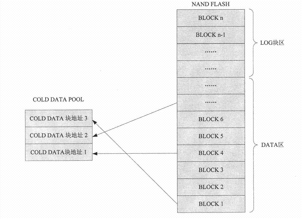
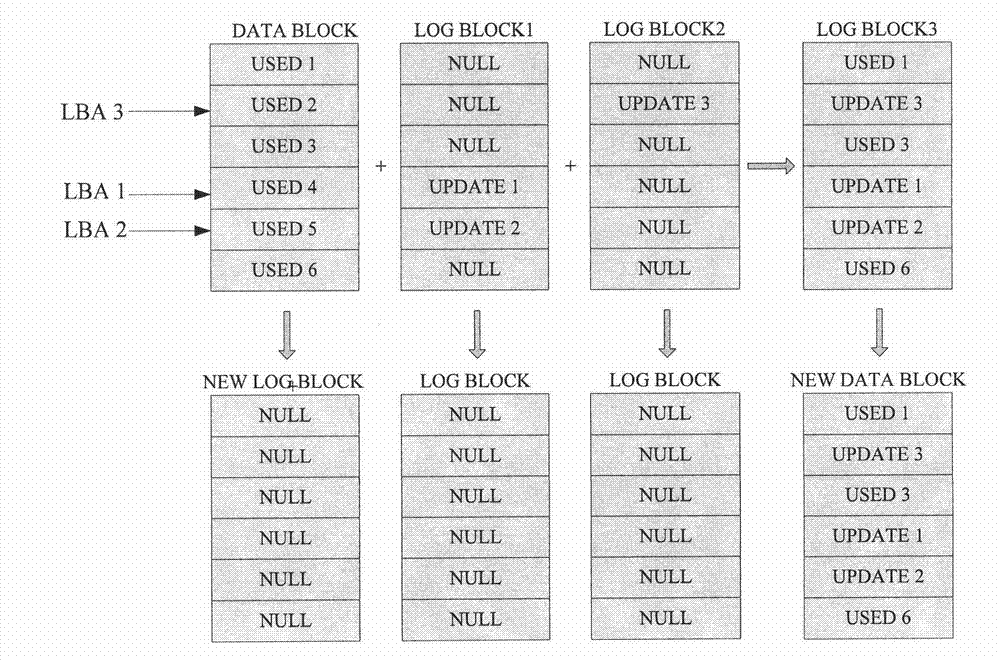
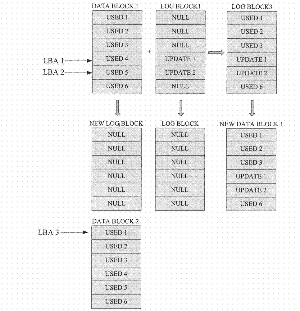
[0030]The invention discloses a method for NAND FLASH to realize balanced loss, which includes a local balanced realization method and a global balanced realization method. In this method, the blocks in NAND FLASH are allocated as LOG blocks according to the total number of NAND FLASH blocks and system performance requirements, and the LOG block with the lowest number of erases and writes is preferentially allocated as the new data for the number of erases and writes of each LOG block. Store blocks to achieve local balance in the LOG block; according to a certain rhythm, record the data blocks with relatively few erasing times in the data block to COLD-DATA-POOL; compare the block with the most erasing times in the LOG block with The erasing times of the block with the least erasing times in COLD-DATA-POOL, when the difference is greater than or equal to a certain threshold, copy the data in the block with the least erasing times in COLD-DATA-POOL to the LOG block The block wi...
PUM
 Abstract
Description
Claims
Application Information