Detection and Classification Method for Surface Defects of Large Aperture Optical Components

A technology of optical components and classification methods, applied in the direction of optical testing flaws/defects, etc., can solve the analysis of difficult-to-absorb defects, non-absorptive defects cannot be applied, and non-absorptive defects are not sensitive, so as to improve the efficiency of inspection and increase the contrast ratio. , the effect of high recognition

Active Publication Date: 2015-08-26
合肥利弗莫尔仪器科技有限公司
View PDF10 Cites 0 Cited by
  • Summary
  • Abstract
  • Description
  • Claims
  • Application Information

AI Technical Summary

Problems solved by technology

[0004] Some defect detection methods commonly used at present, such as high-resolution scattering measurement method, high-resolution fluorescence measurement method, atomic force microscope, scanning tunneling microscope, near-field optical microscope, high-resolution photoacoustic microscope, and various high-resolution photothermal microscopes, etc. , only a certain type of defect can be effectively detected: the high-resolution scattering measurement method is mainly sensitive to the inhomogeneity caused by the optical refractive index or the surface shape defect, and it is difficult to be used for the analysis of the absorption defect
High-resolution fluorescence measurements are good at detecting optically absorbing defects, but are insensitive to non-absorbing defects
Photoacoustic and various photothermal microscopy methods can effectively detect absorption defects, but cannot be applied to non-absorption defects

Method used


Image

  • Detection and Classification Method for Surface Defects of Large Aperture Optical Components
  • Detection and Classification Method for Surface Defects of Large Aperture Optical Components
  • Detection and Classification Method for Surface Defects of Large Aperture Optical Components

Examples


Embodiment Construction

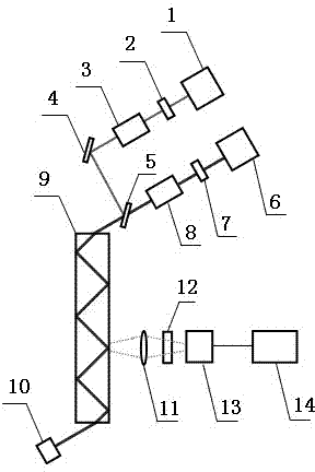
[0031] See figure 1 , a detection and classification device for surface defects of large-aperture optical components:

[0032] It includes a strong lighting source 1, a weak lighting source 6, a strong lighting beam switch 2 arranged at the rear end of the strong lighting light source 1, a weak lighting beam switch 7 arranged at the rear end of the weak lighting light source 6, and a strong lighting beam switch 7 arranged at the rear end of the strong lighting beam switch 2. Lighting beam shaping processing device 3, weak lighting beam shaping processing device 8 arranged at the rear end of weak lighting beam switch 7, high reflection mirror 4 arranged at the rear end of strong lighting beam shaping processing device 3, behind weak lighting beam shaping processing device 8 The dichroic mirror 5 whose reflective surface is arranged relative to the reflective surface of the high reflection mirror 4, the illumination beam absorbing device 10 arranged on the exit side of the rela...


PUM


Abstract

The invention discloses a method and a device for detecting and classifying surface defects of a large-aperture optical element. The large-aperture optical element is irradiated by using a high-intensity light beam and a low-intensity light beam; the high-intensity light beam and an absorption defect interacts to generate fluorescent light; the low-intensity light beam and a non-absorption defect interacts to cause light beam scattering; and information of the absorption defect and information of the non-absorption defect of the large-aperture optical element can be obtained by respectively detecting the fluorescent light and the scattered light. According to the method and the device, by an inner full-reflection type illumination mode, a plurality of regions in the large-aperture optical element are synchronously illuminated and detected, so that the detection efficiency is improved. At the detection end, only the surface defects and sub-surface defects are detected by an imaging system with a small focal depth or a confocal imaging method. The method and the device are suitable for optical lossless flaw detection, optical precision detection, optical microimaging and defect analysis, and in particular suitable for a plurality of fields of surface and sub-surface defect detection of a large-aperture transparent optical element in a high-laser system.

Description

technical field [0001] The invention relates to the field of optical material defect detection, in particular to a method for detecting and classifying surface defects of large-diameter optical elements. Background technique [0002] For many optical materials, such as fused silica glass and KDP crystals, which are commonly used in strong laser systems, surface and subsurface defects and contamination will inevitably be introduced during material processing, such as cutting, grinding, polishing, etc. , so the optical quality of its surface and subsurface is often much worse than the intrinsic properties of related materials, so that the surface and subsurface of related components become the bottleneck limiting the performance of components in many applications, such as the most powerful laser system. Weak link that is easily damaged by laser light. [0003] For the surface and subsurface defects of optical materials, they can usually be divided into absorption defects and ...

Claims


Application Information

Patent Timeline
Patent Type & Authority Patents(China)
IPC IPC(8): G01N21/88
Inventor 陈坚吴周令黄明
Owner 合肥利弗莫尔仪器科技有限公司
Why Eureka
Try Eureka