Device and method for correcting pixel output nonlinear response of image sensor

A non-linear response, image sensor technology, applied in image communication, electrical components, color TV components, etc., can solve the problems of troublesome and difficult realization of layout, achieve small chip area, suppress nonlinear problems, improve The effect of linearity

Active Publication Date: 2013-05-22
NO 771 INST OF NO 9 RES INST CHINA AEROSPACE SCI & TECH
View PDF6 Cites 8 Cited by
  • Summary
  • Abstract
  • Description
  • Claims
  • Application Information

AI Technical Summary

Problems solved by technology

First of all, this method requires the current in the current sink and the current in the current source to match accurately, which is difficult to achieve in engineering; secondly, thi

Method used


Image

  • Device and method for correcting pixel output nonlinear response of image sensor
  • Device and method for correcting pixel output nonlinear response of image sensor
  • Device and method for correcting pixel output nonlinear response of image sensor

Examples


Embodiment Construction

[0042] The present invention will be further described in detail below in conjunction with specific embodiments, which are explanations of the present invention rather than limitations.

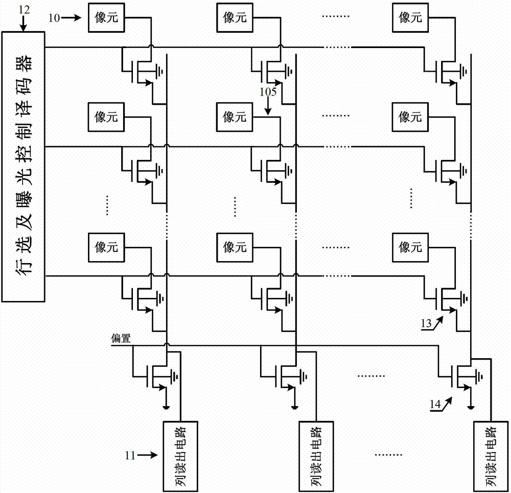
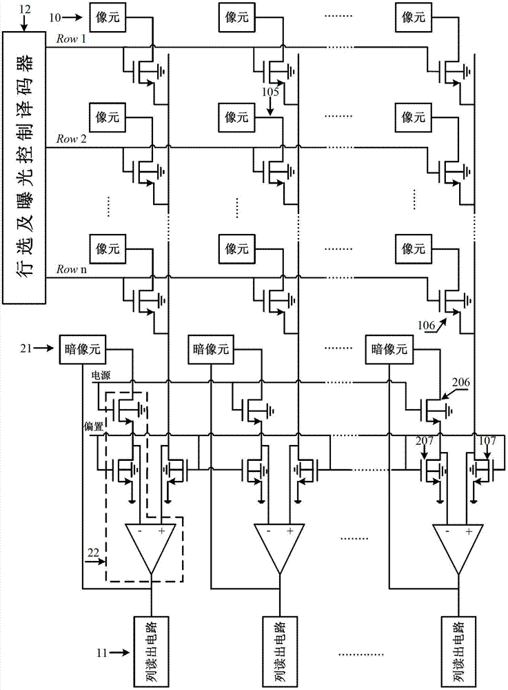
[0043] figure 1Shown is the overall layout structure of a typical CMOS image sensor. The row selection and exposure control decoder 12 generates a row selection signal and an exposure signal. The row selection signal is sent to the row selection switch 106, and the exposure signal is sent to the photosensitive pixel array 10. The pixel array 10 converts optical signals of different intensities into analog electrical signals, and connects them to the column lines through the row selection switch 106, and the column readout circuit 11 receives the signals transmitted by the column lines, and quantizes the analog electrical signals into easy-to-storage , The transmitted digital signal.

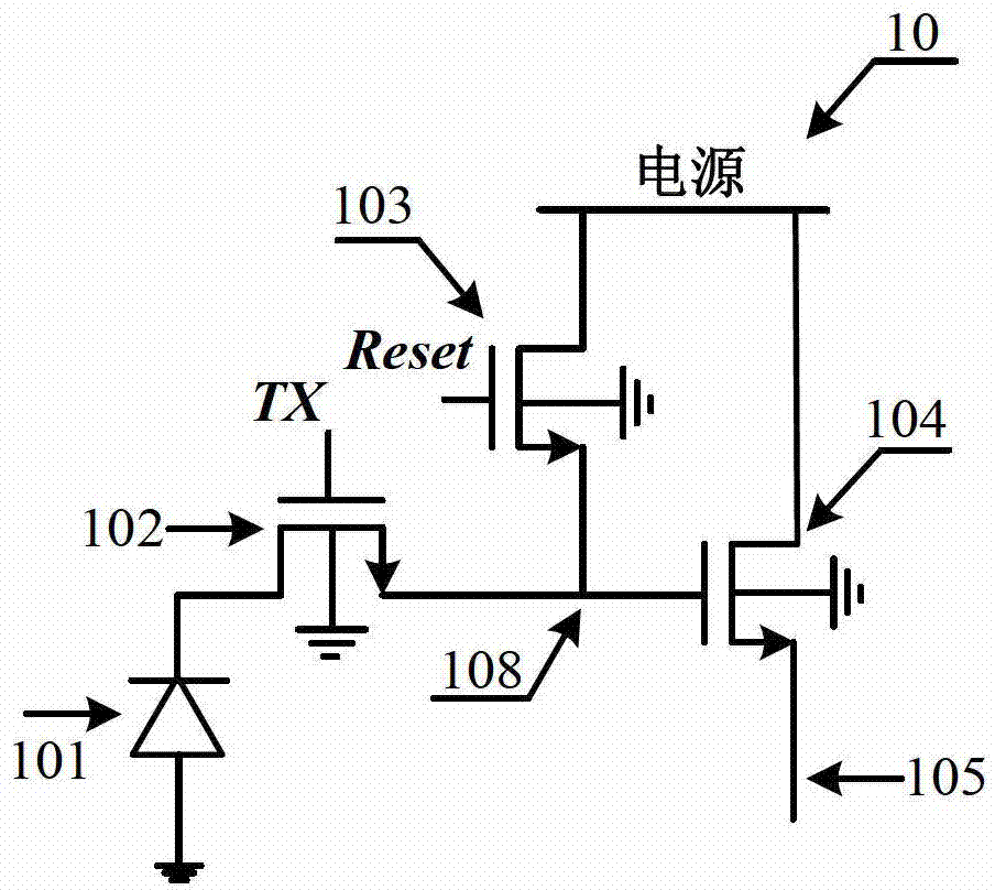
[0044] figure 2 Shown is a single photosensitive pixel circuit of the photosensitive pixel array 10, inclu...


PUM


Abstract

The invention discloses a device and a method for correcting pixel output nonlinear response of an image sensor. The device comprises a photosensitive pixel array, a dark pixel, a photosensitive pixel row selection switch, a dark pixel switch, a photosensitive pixel bias current source, a dark pixel bias current source, a linear circuit, a simulating line reading circuit and a row selection and exposure control decoder. Compared with traditional image sensors, a nonlinear correcting circuit formed by the dark pixel and the linear circuit is added, the correcting circuit occupies smaller chip area, effectively restrains nonlinear problems caused by substrate bias effects, linearity of pixel output signals and imaging quality of image sensors are improved greatly.

Description

technical field [0001] The invention belongs to the technical field of CMOS image sensors, and relates to a correction device and method for nonlinear response of pixel output in an image sensor. Background technique [0002] Image sensors are at the heart of modern electronic imaging systems, including video cameras, digital cameras, copiers, scanners, and more. Image sensors are mainly implemented based on two processes, complementary metal-oxide-semiconductor (CMOS) process and charge-coupled device (CCD) process. [0003] Complementary metal-oxide-semiconductor (CMOS) image sensor technology has developed rapidly with Moore's Law, especially in recent years, driven by the market, key technologies have continuously made breakthroughs, and the signal-to-noise ratio and dynamic range are constantly approaching CCD. Its advantages such as high integration, small size, and low power consumption make CMOS image sensors account for more than 80% of the image sensor market. N-...

Claims


Application Information

Patent Timeline
IPC IPC(8): H04N5/359H04N5/361
Inventor 韩本光郭仲杰汪西虎吴龙胜
Owner NO 771 INST OF NO 9 RES INST CHINA AEROSPACE SCI & TECH
Why Eureka
Try Eureka