Photo spacer and liquid crystal display panel

A liquid crystal display panel, liquid crystal panel technology, applied in the direction of instruments, nonlinear optics, optics, etc., can solve the problems affecting the size of the gap between liquid crystal cells and uneven gap between liquid crystal cells

Active Publication Date: 2013-06-05
SHANGHAI TIANMA MICRO ELECTRONICS CO LTD
View PDF4 Cites 20 Cited by
  • Summary
  • Abstract
  • Description
  • Claims
  • Application Information

AI Technical Summary

Problems solved by technology

[0007] The technical problem to be solved by the present invention is that the photoresist spacers in the seal area (seal area) of the liquid crystal display panel in the prior art are stacked with the conductive gold balls, which affects the size of the gap between the liquid crystal cells and makes the gap between the liquid crystal cells uneven

Method used


Image

  • Photo spacer and liquid crystal display panel
  • Photo spacer and liquid crystal display panel
  • Photo spacer and liquid crystal display panel

Examples


Embodiment Construction

[0027] Several embodiments of the present invention will be listed below, together with the accompanying drawings, component symbols, etc., to describe in detail the composition and effects of the present invention.

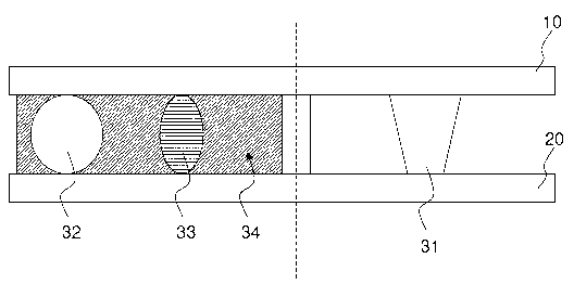
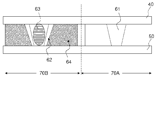
[0028] Please refer to figure 2 and image 3 , figure 2 It is a schematic diagram of the structure of the spacers disposed on the liquid crystal display panel of the present invention. image 3 It is an end view of the spacer disposed on the sealant of the liquid crystal display panel of the present invention. The structure of the liquid crystal display panel 70 of this embodiment includes an upper substrate (which may be a color filter substrate) 40, a lower substrate (which may be a thin film transistor substrate) 50 parallel to the upper substrate 40, and arranged on the upper substrate. A liquid crystal layer (not shown) between the substrate 40 and the lower substrate 50 . The liquid crystal display panel 70 includes a working area 70A and a sealant ar...


PUM


Abstract

The invention provides a photo spacer and a liquid crystal display panel. The photo spacer is used for a display panel, and the display panel comprises an upper substrate, a lower substrate, a plurality of liquid crystal boxes, a plurality of fist photo spacers, a plurality of second photo spacers, a plurality of conducting particles and seal. The first photo spacers are arranged in a first seal area of the display panel and comprise first through holes, the conducting particles are arranged in the seal area corresponding between the upper substrate and the lower substrate, and the second photo spacers are correspondingly arranged in a first active area of the display panel. The seal is filled between the first photo spacers and the conducting particles, and when the conducting particles vertically correspond to the first photo spacers, the conducting particles are embedded in the through holes. The photo spacer can replace a silicon photo spacer, and the problem that spaces of the liquid crystal boxes are influenced due to stacking of the photo spacers and complete cycle conducting golden spacers is solved.

Description

technical field [0001] The invention relates to the field of liquid crystal display technology, in particular to a spacer for a liquid crystal display panel and a liquid crystal display panel. [0002] Background technique [0003] The liquid crystal display panel is mainly composed of a lower substrate (which may be a thin film transistor substrate), an upper substrate (which may be a color filter substrate) and a liquid crystal layer filled between the two substrates. In order to ensure stable display quality and sufficient supporting force, spacers must be uniformly arranged between the lower substrate and the upper substrate so as to maintain a fixed cell gap between the two substrates. [0004] Please refer to figure 1 , figure 1 It is a schematic diagram of a liquid crystal display panel using known spacers. Such as figure 1 A liquid crystal display panel usually includes an upper substrate 10 , a lower substrate 20 , a first spacer 31 , a second spacer 32 , condu...

Claims


Application Information

Patent Timeline
Patent Type & Authority Applications(China)
IPC IPC(8): G02F1/1339G02F1/1333
Inventor 刘青刚黄贤军
Owner SHANGHAI TIANMA MICRO ELECTRONICS CO LTD
Why Eureka
Try Eureka