

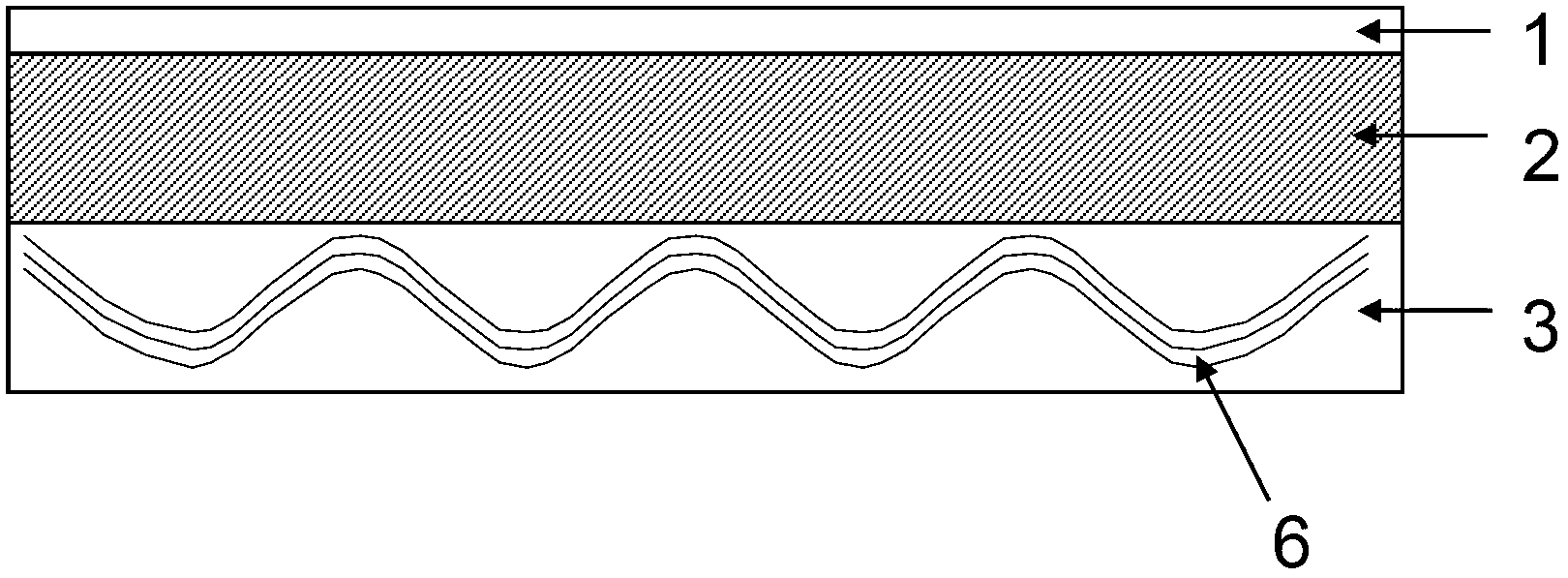
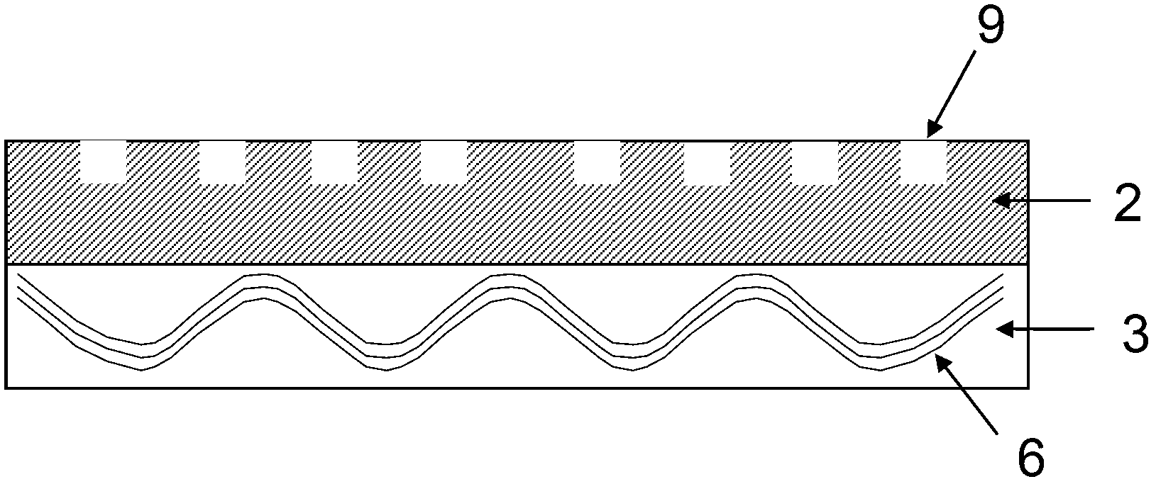
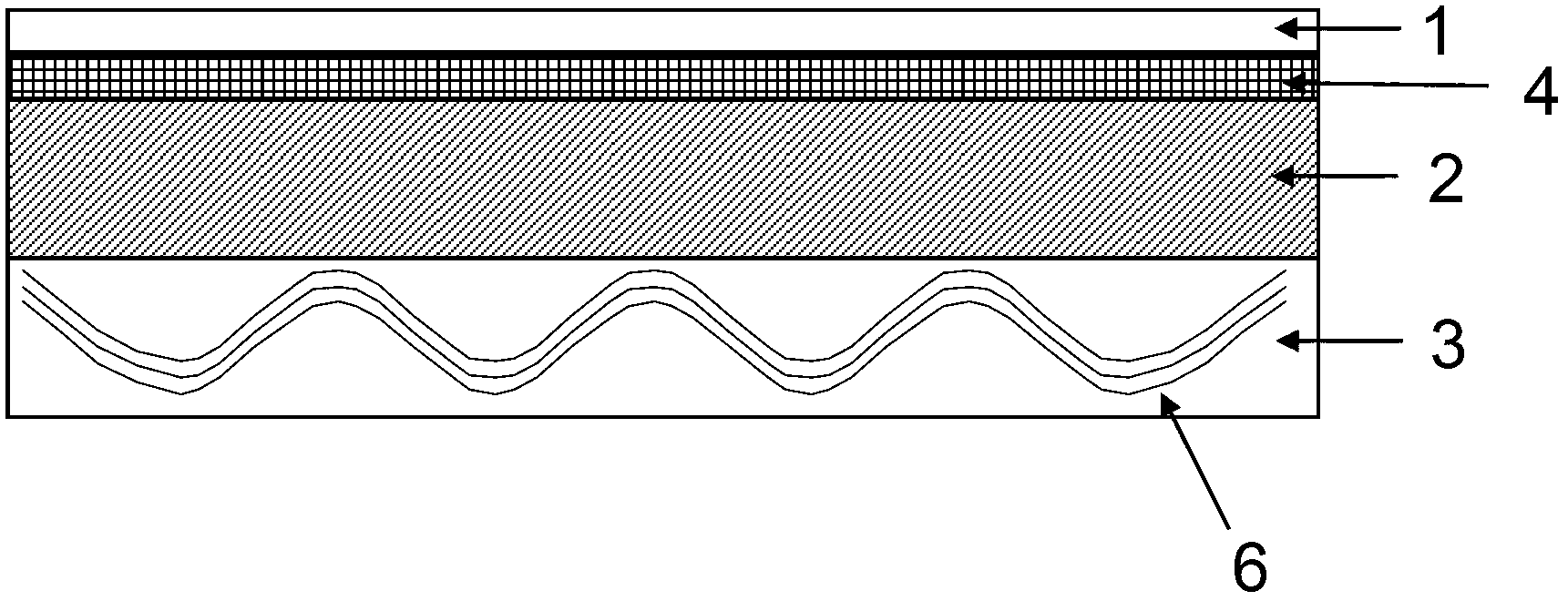
Composite build-up material for embedding of circuitry
A technology of circuits and mixtures, applied in the directions of printed circuits, printed circuits, printed circuit manufacturing, etc., can solve problems such as uneven laser ablation
- Summary
- Abstract
- Description
- Claims
- Application Information
AI Technical Summary
Problems solved by technology
Method used
Image

Examples
Embodiment
[0143] Preparation of resin powders for layers (2) and (3)
[0144] The resin components listed in Table 1 were weighed in the amounts indicated and thoroughly mixed together in polyethylene bags.
[0145] Table 1: Components for resin powder preparation of resin layers (2) and (3)
[0146] components
Quantity (g)
Multifunctional solid epoxy resin
480
Bakelit PF 0790 K03
180
Submicron Size Silicon Oxide
338
Total:
998
[0147] Use dicyclopentadienyl-bridged polyfunctional solid epoxy resin, Bakelit PF 0790 K03, which is a phenolic-based phenolic resin (CAS-no.9003-35-4), and has a 0.3 micron average Submicron sized silica fillers in particle size and spherical particle shape are used as raw materials. The mixed dielectric components were then extruded on a 19 mm-hole, 5-zone, 24 l / d twin-screw extruder produced by OMC, Italy and equipped with a screw with maximum number of mixing elements. The barrel temperat...
PUM
| Property | Measurement | Unit |
|---|---|---|
| thickness | aaaaa | aaaaa |
| thickness | aaaaa | aaaaa |
| thickness | aaaaa | aaaaa |
Abstract
Description
Claims
Application Information