Thin film transistor array panel and liquid crystal display device

A technology of liquid crystal display device and thin film transistor, which is applied in static indicators, instruments, nonlinear optics, etc., can solve problems such as the inability to realize narrow frames well, achieve frame area saving, avoid threshold voltage drift, and simple structure Effect

Active Publication Date: 2016-05-18
SHANGHAI TIANMA MICRO ELECTRONICS CO LTD
View PDF5 Cites 0 Cited by
  • Summary
  • Abstract
  • Description
  • Claims
  • Application Information

AI Technical Summary

Problems solved by technology

Narrow bezels are still not well implemented as the number of gate line leads is also large

Method used


Image

  • Thin film transistor array panel and liquid crystal display device
  • Thin film transistor array panel and liquid crystal display device
  • Thin film transistor array panel and liquid crystal display device

Examples


Embodiment Construction

[0029] In order to make the above objects, features and advantages of the present invention more comprehensible, specific implementations of the present invention will be described in detail below in conjunction with the accompanying drawings.

[0030] In the following description, many specific details are set forth in order to fully understand the present invention, but the present invention can also be implemented in other ways than those described here, so the present invention is not limited by the specific embodiments disclosed below.

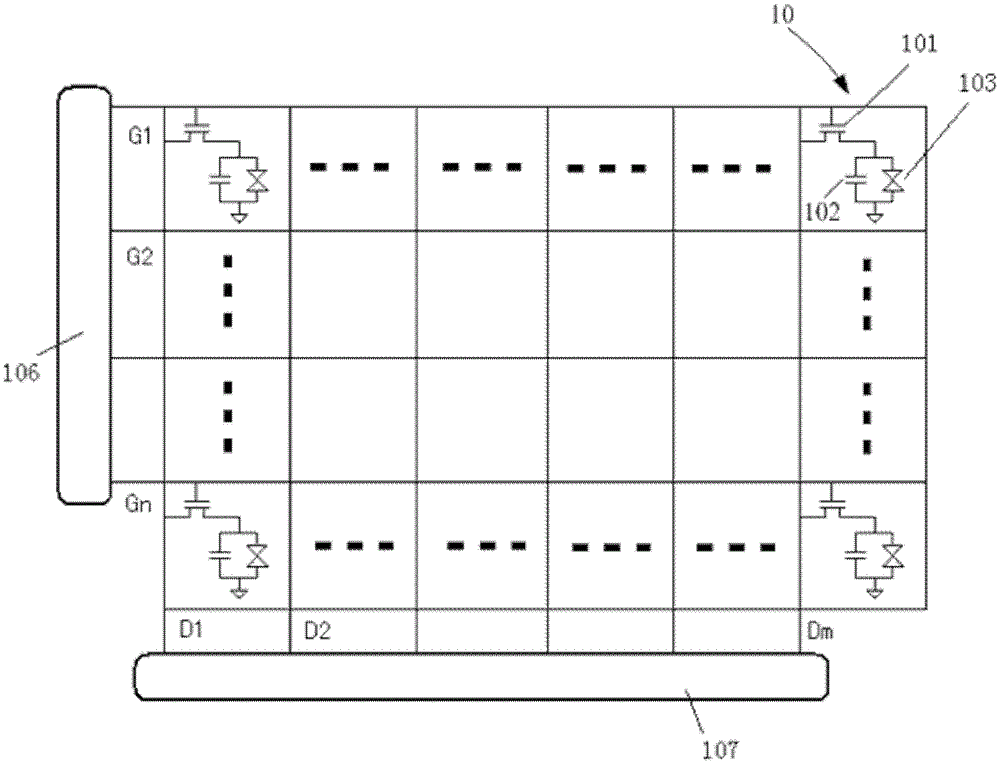
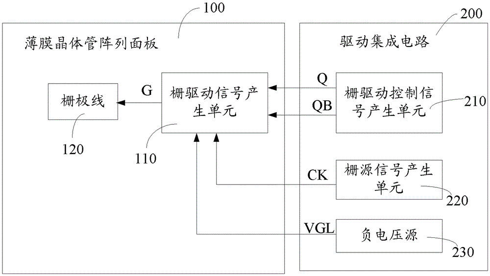
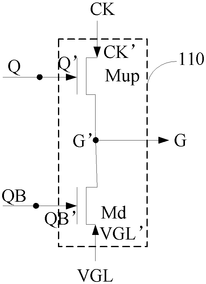
[0031] In order to realize the narrow frame design of the display panel, the present invention provides a thin film transistor array panel and a liquid crystal display device, wherein: the first gate drive control signal, the second gate drive control signal, and the gate-source signal received by the gate drive signal generating unit The negative voltage signal and the negative voltage signal are generated outside the thin film transistor...


PUM


Abstract

Disclosed are a thin film transistor array panel and a liquid crystal display (LCD) device. The thin film transistor array panel comprises a plurality of gate lines, data lines, a plurality of pixel units and a multistage gate driving signal generation unit, wherein the plurality of gate lines and the data lines are perpendicular to each other. Each pixel unit comprises at least one thin film transistor, the gate lines are connected with a grid electrode of the thin film transistor, and the data lines are connected with a source electrode of the thin film transistor. The multistage gate driving signal generation unit is connected with the gate lines and is used for receiving a first grid driving control signal, a second grid driving control signal, a gate source signal and a negative voltage signal and supplying gate driving signals to the gate lines. The phase position of the first grid driving control signal is opposite to the phase position of the second grid driving control signal. By means of the thin film transistor array panel and the LCD device, a narrow frame of the thin film transistor array panel can be achieved.

Description

technical field [0001] The invention relates to the technical field of liquid crystal manufacturing, in particular to a thin film transistor array panel and a liquid crystal display device. Background technique [0002] In a liquid crystal display (LCD) or other flat-panel displays with a similar structure, such as e-books, organic light-emitting diode flexible displays, etc., the gate lines are horizontally arranged as the row driving lines in the layout of the liquid crystal pixel array. [0003] Taking a thin film transistor liquid crystal panel (TFT-LCD) as an example, it displays images through a matrix of liquid crystal pixels. See figure 1 , figure 1 It is a structural diagram of a TFT-LCD panel in the prior art, including multiple sub-pixel units, multiple gate lines G1, G2...Gn, and multiple data lines D1, D2...Dm connected thereto. Each sub-pixel unit includes a thin film transistor (TFT), a storage capacitor, a liquid crystal capacitor, etc., and the gate of th...

Claims


Application Information

Patent Timeline
Patent Type & Authority Patents(China)
IPC IPC(8): G02F1/1362G02F1/1368G02F1/133G09G3/36
Inventor 李嘉灵张良吴天一
Owner SHANGHAI TIANMA MICRO ELECTRONICS CO LTD
Why Eureka
Try Eureka