Supercharge Your Innovation With Domain-Expert AI Agents!

Ways to avoid sharp metal corners

A sharp corner and metal technology, applied in the field of avoiding metal sharp corners, to achieve the effect of no sharp corners

Active Publication Date: 2015-10-14
SHANGHAI HUAHONG GRACE SEMICON MFG CORP
View PDF3 Cites 0 Cited by
  • Summary
  • Abstract
  • Description
  • Claims
  • Application Information

AI Technical Summary

Problems solved by technology

[0005] The technical problem to be solved by the present invention is to provide a method for avoiding metal sharp corners, by using a wet etching with a high selectivity ratio to form another height difference in the original height difference region, thereby avoiding the possible occurrence of the original sharp corners place, thereby eliminating the possibility of forming sharp corners, thereby solving the problem of tip discharge caused by sharp corners of metal wires

Method used


Image

  • Ways to avoid sharp metal corners
  • Ways to avoid sharp metal corners
  • Ways to avoid sharp metal corners

Examples


Embodiment Construction

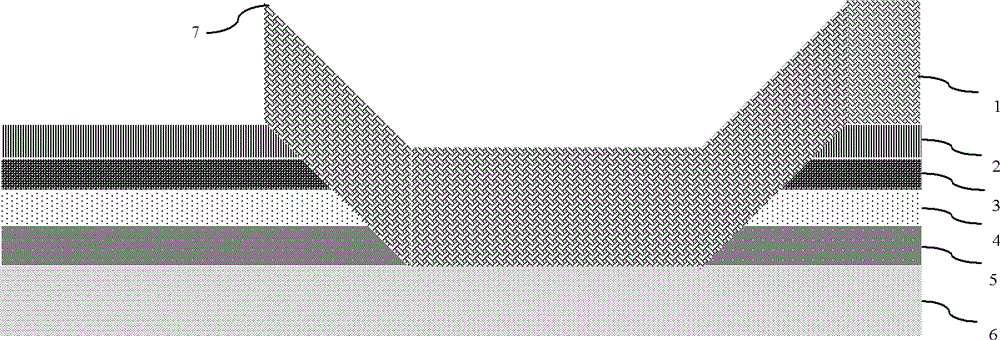
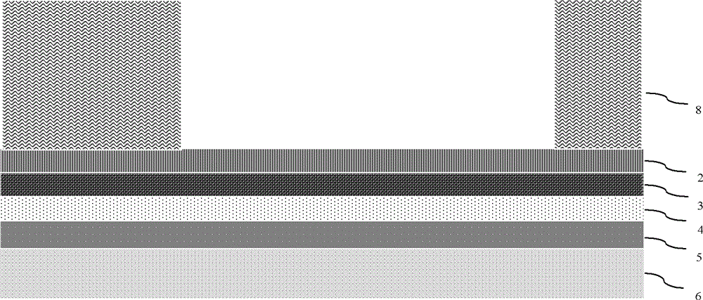
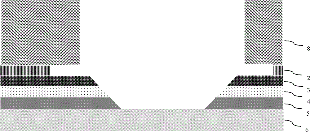
[0037] The method for avoiding metal sharp corners in the preparation of insulated gate bipolar transistors of the present invention comprises the steps of:

[0038] (1) grow several layers of oxide films on the silicon substrate 6, the specific steps are as follows:

[0039] like figure 2 As shown, different doping concentrations, film forming temperatures and film forming methods are used on the silicon substrate 6 to grow the following oxide films:

[0040] ①Use subatmospheric pressure chemical vapor deposition first, and deposit a layer of subatmospheric phosphorus doped silicon oxide film 5 (first oxide film) grown at 480°C with a doping concentration of 3% at 1 micron under a pressure of 200 Torr. );

[0041] ② On the basis of step ①, use high-density plasma chemical vapor deposition to grow a layer of 0.7 micron high-density plasma-enhanced phosphorus-doped silicon oxide grown at 380°C with a doping concentration of 4% under a pressure of 10 mTorr Film 4 (first oxid...


PUM

PropertyMeasurementUnit
thicknessaaaaaaaaaa
thicknessaaaaaaaaaa

Abstract

The method discloses a method for avoiding generating metal sharp angles. The method comprises the steps of growing a plurality of layers of oxidation films on a silicon substrate; forming groove appearance by etching; growing metal connecting lines; and performing metal connecting line etching. High-low difference appearance is formed by enabling a second oxide film or a dielectric film to undergo transverse etching towards two sides, enabling original groove corners to respectively expand towards two sides so as to avoid formation of regions where the metal sharp angles occur originally. Accordingly, a metal wire in an insulated gate bipolar transistor device has no sharp angles, and the problem of device invalidation caused by discharge at a metal point is solved.

Description

technical field [0001] The invention relates to a method for improving metal sharp corners in the field of semiconductors, in particular to a method for avoiding metal sharp corners. Background technique [0002] Insulated gate bipolar transistor (Insolated Gate Bipolar Transistor, IGBT) is a device composed of a MOSFET and a bipolar transistor. Its input is a MOSFET and its output is a PNP transistor. It combines the advantages of these two devices. It not only has the advantages of small driving power and fast switching speed of MOSFET devices, but also has the advantages of low saturation voltage and large capacity of bipolar devices. Therefore, it has been more and more widely used in modern power electronics technology. [0003] In the subsequent metal wire fabrication process of the IGBT, due to the existence of the groove in the front layer, the metal wire is very easy to form a sharp angle on the edge of the groove, that is, a very sharp angle will be formed in the a...

Claims


Application Information

Patent Timeline
Patent Type & Authority Patents(China)
IPC IPC(8): H01L21/3213H01L21/311H01L21/331
Inventor 郁新举
Owner SHANGHAI HUAHONG GRACE SEMICON MFG CORP
Features
  • R&D
  • Intellectual Property
  • Life Sciences
  • Materials
  • Tech Scout
  • Unparalleled Data Quality
  • Higher Quality Content
  • 60% Fewer Hallucinations
Learn More