
Processing method of opening cover of pcb board

A PCB board and processing method technology, applied in the field of PCB board processing, can solve the problems of uneven PCB board edges, scrapped PCB boards, and increased production costs, so as to achieve smooth and dust-free cutting edges, reduce production costs, and improve cutting efficiency. quality effect

Active Publication Date: 2015-12-23
HANS CNC SCI & TECH
View PDF12 Cites 0 Cited by
  • Summary
  • Abstract
  • Description
  • Claims
  • Application Information

AI Technical Summary

Problems solved by technology

[0003] The traditional PCB board opening adopts mold punching technology for half-cutting, which may easily cause uneven edges of the PCB board, or damage the bottom board, etc., causing the PCB board to be scrapped
Moreover, different PCB boards need to be equipped with different molds. If the upgrade file of the same type of PCB board is changed, the mold needs to be changed, which increases the production cost.

Method used


Image

  • Processing method of opening cover of pcb board
  • Processing method of opening cover of pcb board

Examples


Embodiment Construction

[0019] In order to facilitate the understanding of the present invention, the present invention will be described more fully below with reference to the associated drawings. Preferred embodiments of the invention are shown in the accompanying drawings. However, the present invention can be embodied in many different forms and is not limited to the embodiments described herein. On the contrary, these embodiments are provided to make the understanding of the disclosure of the present invention more thorough and comprehensive.

[0020] It should be noted that when an element is referred to as being “fixed” to another element, it can be directly on the other element or there can also be an intervening element. When an element is referred to as being "connected to" another element, it can be directly connected to the other element or intervening elements may also be present. The terms "vertical," "horizontal," "left," "right," and similar expressions are used herein for purposes ...


PUM


Abstract

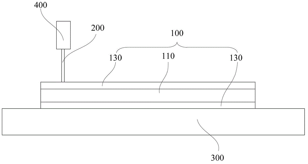
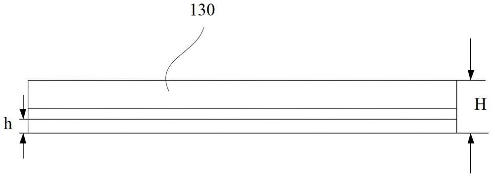
The invention discloses a processing method of a PCB (Printed Circuit Board) open cover. The processing method comprises the following steps: presetting the shape of the open cover area of the PCB; placing the PCB on a processing platform; cutting along the border of the open cover area by utilizing a laser beam, wherein the power of the laser beam is 3 watts to 10 watts, the movement speed of the laser beam relative to the PCB is 100 mm / s to 400mm / s, the pulse power of the laser beam is 5 khz to 150 khz and the pulse time is 1 microsecond to 5 microseconds. The processing method of the PCB open cover is used for cutting along the border of the open cover area by utilizing the laser beam, so that the processing depth of the PCB can be controlled and the cutting edge is flat and dust-free, and therefore, the cutting quality is improved, the production cost is reduced and the competitive power of the PCB is improved.

Description

【Technical field】 [0001] The invention relates to a processing method of a PCB board, in particular to a processing method of a PCB board processed by laser. 【Background technique】 [0002] PCB board opening processing is an important process in PCB board factories. Due to the rapid changes in the electronic product market, the replacement time of new product models is accelerated, and the competition among circuit board companies is becoming more and more serious. In order to obtain more orders, various companies Both speed up the delivery of samples. [0003] The traditional PCB cover opening adopts mold punching technology for half-cutting, which may easily cause uneven edges of the PCB board, or damage the bottom board, resulting in the scrapping of the PCB board. Moreover, different PCB boards need to be equipped with different molds. If the upgrade file of the same type of PCB board is changed, the mold needs to be changed, which increases the production cost. 【Cont...

Claims


Application Information

Patent Timeline
Patent Type & Authority Patents(China)
IPC IPC(8): B23K26/38B23K26/08B23K37/04B23K26/36
Inventor 范永闯高云峰
Owner HANS CNC SCI & TECH
Learn More