Customized using backside approach IC chip

一种集成电路、背面的技术,应用在使用背面接近的集成电路芯片定制领域,能够解决掩模组昂贵、不完全编程、结构复杂性增加等问题

Active Publication Date: 2016-08-10
QUALCOMM INC
View PDF3 Cites 0 Cited by
  • Summary
  • Abstract
  • Description
  • Claims
  • Application Information

AI Technical Summary

Problems solved by technology

This problem can be solved using more complex metallization patterns, but it can be seen that the complexity of the overall structure is also significantly increased, and this method will not be carried out because the mask sets used in the production are expensive
[0008] Furthermore, using standard programming techniques, the amount of voltage or current that can be applied to a programming signal is limited because programming is done from pads on the front side that are not necessarily in close proximity to the element to be programmed, and Programming signals may be conducted through very long signal path conductors to programmable elements
This often results in incomplete or invalid programming, as applying the specified programming voltage or current may not be sufficient to cause the corresponding programmable element to change state

Method used


Image

  • Customized using backside approach IC chip
  • Customized using backside approach IC chip
  • Customized using backside approach IC chip

Examples


Embodiment Construction

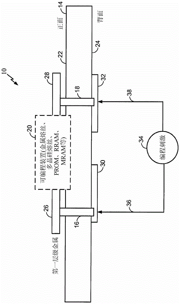
[0022] see now figure 1 ,exist figure 1 An example of an embodiment 10 of an integrated circuit structure in which backside TSV programming can be implemented is shown in . Note that although illustrative embodiment 10 is described in terms of through-silicon vias, or TSVs, the examples are not intended to be limited to silicon substrates or TSVs, but may be equally advantageously practiced with other semiconductor processes, materials, and the like. For example, substrate 14 may be any suitable substrate material, such as gallium arsenide, indium phosphide, silicon germanium, indium gallium arsenide, silicon-on-glass, silicon-on-sapphire, silicon-on-ceramic, glass, sapphire, ceramic, Laminates, Bismaleimide Triazine (BT), FR4, Epoxy, Epoxy Blends, etc. Additionally, while TSVs are described in the illustrated embodiments, any suitable via compatible with the substrate material may be used.

[0023] The word "example" or "exemplary" is used to mean "serving as an example, i...


PUM


Abstract

An integrated circuit, a method for manufacturing an integrated circuit product, and a method for customizing an integrated circuit are disclosed. Integrated circuit elements are formed on the front side of the substrate, including programmable elements such as fuses, PROM, RRAM, MRAM, and the like. Vias are formed through the substrate from the front side of the substrate to the back side of the substrate to establish conductive paths from the back side to at least some of the programmable elements. A programming stimulus is applied to at least some of the vias from the backside to program at least some of the frontside programmable elements.

Description

technical field [0001] Various embodiments described herein relate generally to improvements in semiconductor fabrication processes, products, and devices, and more particularly, to methods for fabricating programmable semiconductor integrated circuits, for performing programmable semiconductor integrated circuits on the programmable semiconductor integrated circuits Methods of programming, and integrated circuit products made therefrom. Background technique [0002] As semiconductor integrated circuit products become more complex, manufacturers continue to find ways to increase the usability of specific circuit designs without having to continually redesign circuits with common components. For example, circuits often have different circuit elements on a single chip that can be enabled by activating programmable elements such as fuses, antifuses, programmable read-only memory (PROM), resistive RAM, etc. RAM (RRAM), Magnetic Random Access Memory (MRAM), etc. [0003] At the...

Claims


Application Information

Patent Timeline
Patent Type & Authority Patents(China)
IPC IPC(8): H01L21/768H01L23/48H01L23/525G11C17/16G11C13/00G11C11/16
CPCG11C11/16G11C13/0002G11C17/16H01L23/481H01L23/5256H01L2924/0002H01L2924/00H01L21/768H01L23/48H01L21/76898
Inventor 丹尼尔·W·佩里时群·萨姆·顾
Owner QUALCOMM INC
Why Eureka
Try Eureka