Low-color-difference touch substrate and manufacturing method thereof

A manufacturing method and chromatic aberration technology, applied to instruments, electrical digital data processing, input/output process of data processing, etc., can solve problems such as increasing manufacturing costs, color distortion, and affecting display quality, so as to reduce production costs and improve chromatic aberration Effect

Inactive Publication Date: 2013-07-10
BAY PRECISION
View PDF3 Cites 5 Cited by
  • Summary
  • Abstract
  • Description
  • Claims
  • Application Information

AI Technical Summary

Problems solved by technology

[0002] Common touch panels are mainly divided into two types: resistive and capacitive, both of which form a conductive film on a transparent substrate to sense the selected position. Among them, the conductive film of the capacitive type is distributed in a pattern, which is prone to light transmittance. Unevenness and chromatic aberration make the outline of conductive film graphics obvious. In addition, the touch panel is assembled with the display and covers the front side, which will also affect the display quality and cause color distortion
On the other hand, in the process of manufacturing the touch panel, part of the film layer is formed by sputtering, which uses several targets at the same time, thus increasing the manufacturing cost

Method used


Image

  • Low-color-difference touch substrate and manufacturing method thereof
  • Low-color-difference touch substrate and manufacturing method thereof
  • Low-color-difference touch substrate and manufacturing method thereof

Examples


Embodiment Construction

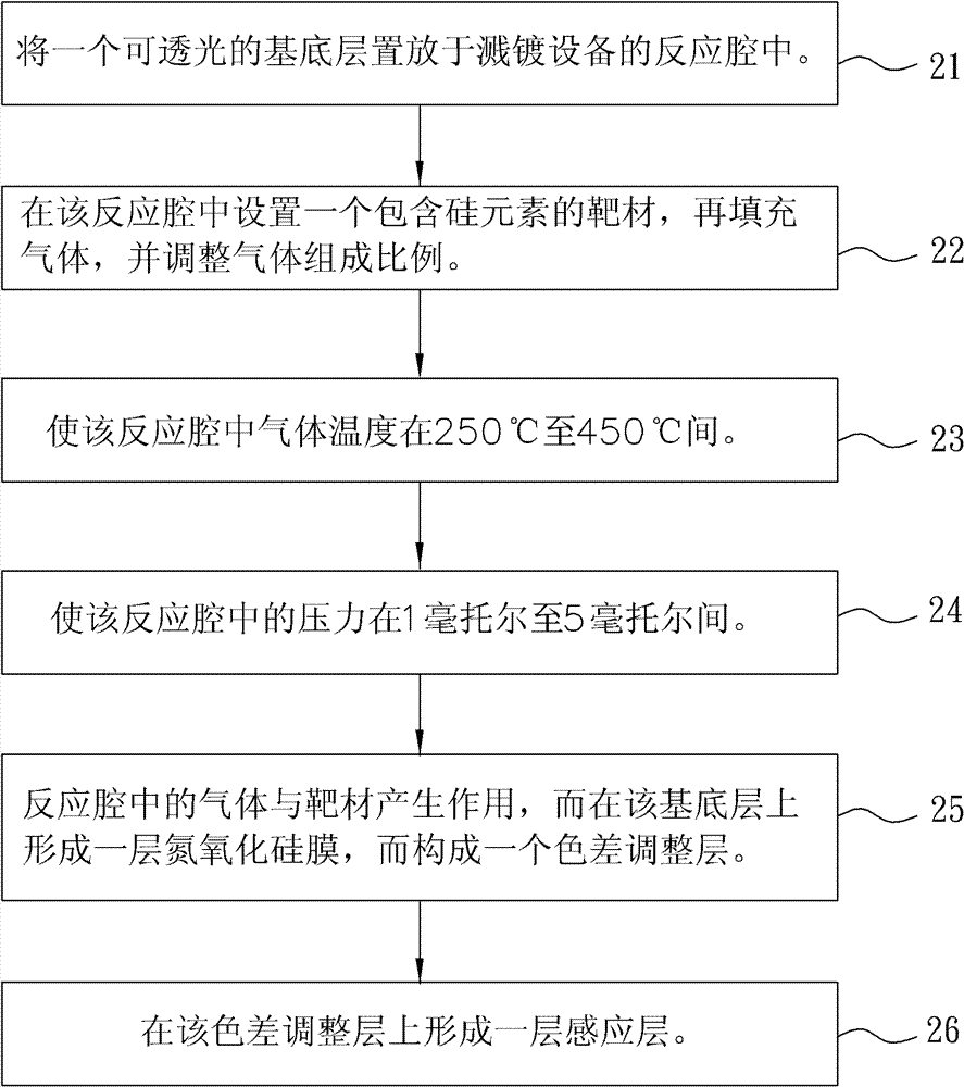
[0027] The present invention will be described in detail below with reference to the accompanying drawings and three embodiments. It should be noted that in the following description, similar elements are denoted by the same numerals.

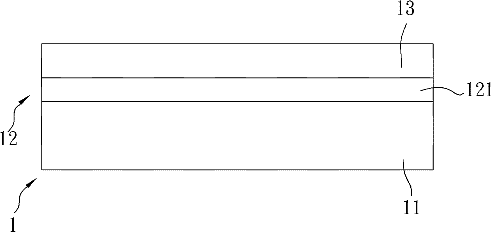
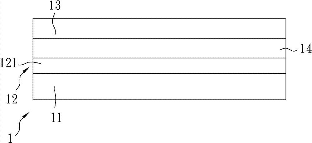
[0028] refer to figure 1 , 2 , the first preferred embodiment of the manufacturing method of the low color difference touch substrate of the present invention is used to form a low color difference touch substrate 1 . The low-color-difference touch substrate 1 includes a light-transmittable base layer 11 , a color-difference adjustment layer 12 covered on the base layer 11 , and a sensing layer 13 covered on the color-difference adjustment layer 12 .

[0029] The base layer 11 of this embodiment is a light-transmitting transparent glass plate. The color difference adjustment layer 12 is transparent and includes a silicon nitride oxide film 121 coated on the base layer 11 . The silicon oxynitride film 121 is made of silicon oxynitride (SiON)....


PUM

PropertyMeasurementUnit
Thicknessaaaaaaaaaa

Abstract

The invention discloses a low-color-difference touch substrate and a manufacturing method thereof. The low-color-difference touch substrate comprises a non-light-tight base layer, a color difference adjustment layer arranged on the base layer in a non-light-tight way, and a sensing layer arranged on the color difference adjustment layer in conductive and non-light-tight ways, wherein the color difference adjustment layer comprises a silicon oxynitride film. As the silicon oxynitride film is arranged between the sensing layer and the base layer, the color difference between the base layer and the sensing layer can be reduced and improved by the silicon oxynitride film.

Description

technical field [0001] The invention relates to a light-transmitting plate, in particular to a low-color-difference touch substrate and a manufacturing method thereof. Background technique [0002] Common touch panels are mainly divided into two types: resistive and capacitive, both of which form a conductive film on a transparent substrate to sense the selected position. Among them, the conductive film of the capacitive type is distributed in a pattern, which is prone to light transmittance. Unevenness and chromatic aberration make the pattern of the conductive film obvious. In addition, the touch panel is assembled with the display and covers the front side, which also affects the display quality and causes color distortion. On the other hand, in the process of manufacturing the touch panel, some film layers are formed by sputtering, which uses several target materials at the same time, thus increasing the manufacturing cost. Contents of the invention [0003] The objec...

Claims


Application Information

Patent Timeline
IPC IPC(8): G06F3/041
Inventor 简谷卫黄导阳辜建烨叶国顺黄圣涵
Owner BAY PRECISION
Why Eureka
Try Eureka