Three-dimensional imaging method and device utilizing planar lightwave circuit

A planar optical waveguide and stereoscopic imaging technology, which is applied in the direction of optical guide, stereoscopic system, stereophotography, etc., can solve the problems of real-time digital acquisition, processing, storage, transmission and display difficulties, and achieve the suppression of smear, fast and simplified images Effects of Illumination Optics

Active Publication Date: 2013-07-17
李志扬
View PDF3 Cites 67 Cited by
  • Summary
  • Abstract
  • Description
  • Claims
  • Application Information

AI Technical Summary

Problems solved by technology

However, for large objects, the holographic interference fringes are on the sub-micron scale, which is far smaller than the pixel size of flat-panel displays; at the same time, massive interference fringe data brings great difficulties to real-time digital acquisition, processing, storage, transmission and display

Method used


Image

  • Three-dimensional imaging method and device utilizing planar lightwave circuit
  • Three-dimensional imaging method and device utilizing planar lightwave circuit
  • Three-dimensional imaging method and device utilizing planar lightwave circuit

Examples


Embodiment Construction

[0049] The present invention will be described in detail below with reference to the accompanying drawings.

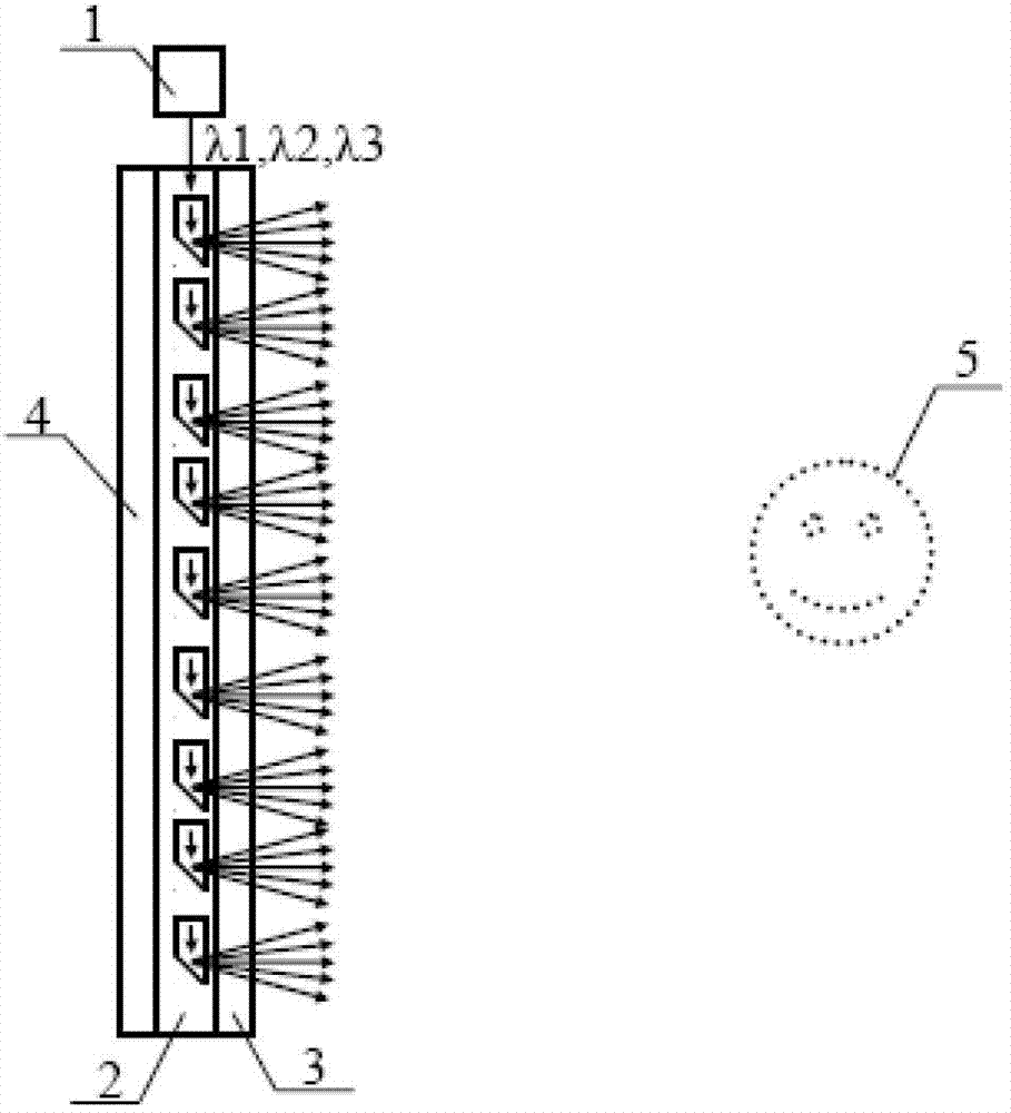
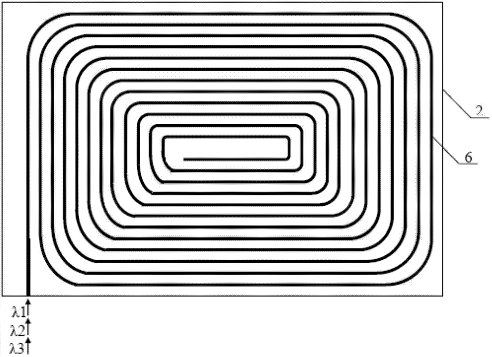
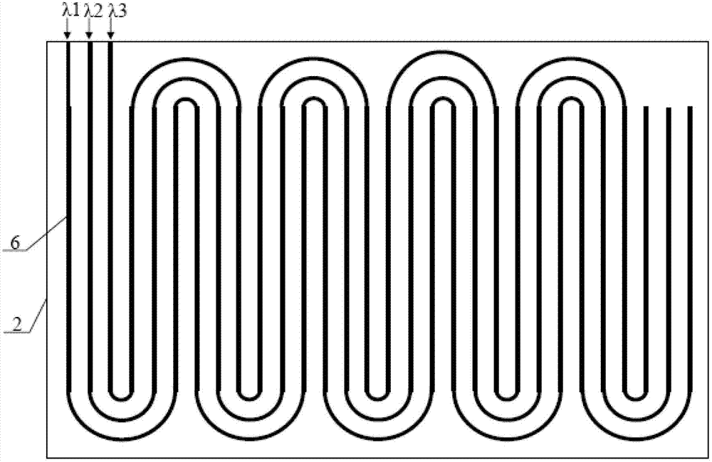
[0050] refer to figure 1 , the three-dimensional display screen of the present invention is composed of a coherent light source 1, a planar optical waveguide circuit 2, a conductive glass front panel 3 and a back drive circuit 4, and the conductive glass front panel 3 and the back drive circuit 4 respectively cover both sides of the planar optical waveguide circuit 2 . further reference Figure 2-7 , the planar optical waveguide circuit 2 includes the trunk optical waveguide 6 and the branch optical waveguide 7 .

[0051] The trunk optical waveguide 6 can adopt either a serial layout or a parallel layout.

[0052] The trunk optical waveguide 6 adopting a serial layout is composed of a single or three optical waveguides, and the single or three optical waveguides uniformly cover the entire planar optical waveguide circuit 2 in a zigzag layout or a spiral layout.

[...


PUM


Abstract

The invention discloses a three-dimensional imaging method and a device utilizing a planar lightwave circuit. The three-dimensional imaging method includes that coherent light emitted from coherent light source is converted into a two dimensional point light source array; the position of every point light source in the two dimensional point light source array is randomly distributed; three-dimensional images are discretized into a large amount of vexel; the vexel is divided into a plurality of groups from high to low according to the brightness; a phase regulating amplitude of the point light source is calculated according to the distance between every point light source and every vexel of every group to enable the lightwave from every point light source to be in the same phase when reaches the vexel; every point light source is accumulated as a complex amplitude regulation amplitude for generating every vexel; and an amplitude regulator and a phase regulator of every point light source are driven to generate every group of vexel based on constructive interference. The imaging device is formed by coherent light source, the planar lightwave circuit, a conductive glass front panel and a back driving circuit. The three-dimensional imaging method and the device utilizing the planar lightwave circuit are capable of being widely applied to the fields of three-dimensional display of a computer and a television, three-dimensional human-machine exchange, robot vision and the like.

Description

technical field [0001] The invention belongs to the technical field of three-dimensional imaging, and in particular relates to a three-dimensional imaging method and device using a planar optical waveguide circuit. Background technique [0002] Three-dimensional display can be divided into pseudo three-dimensional display and true three-dimensional display. The former is a stereoscopic display based on binocular parallax, which presents two pictures with different viewing angles to the left and right eyes of the observer, making them produce stereoscopic illusions, and long-term viewing is likely to cause fatigue. The latter directly forms a real three-dimensional image in the air, and the observer does not need to wear any auxiliary glasses, making viewing more comfortable and natural. [0003] True three-dimensional stereoscopic display can be realized by non-coherent methods, such as integrated imaging technology and volume imaging technology, or by coherent methods, suc...

Claims


Application Information

Patent Timeline
Patent Type & Authority Applications(China)
IPC IPC(8): G02B27/22G03B35/00H04N13/04
CPCG02B6/0035G02B6/0053G02B30/56G03B35/24G03H1/2294G03H2001/0224G03H2223/16G03H2225/33H04N13/305
Inventor 李志扬
Owner 李志扬
Why Eureka
Try Eureka