Simulation method and device for chip surface morphology

A surface topography and chip technology, applied in the field of chip surface topography simulation, can solve problems such as large errors, avoid wrong conclusions, and improve prediction accuracy and accuracy

Active Publication Date: 2013-07-31
INST OF MICROELECTRONICS CHINESE ACAD OF SCI
View PDF3 Cites 18 Cited by
  • Summary
  • Abstract
  • Description
  • Claims
  • Application Information

AI Technical Summary

Problems solved by technology

[0005] The present invention provides a method and device for simulating the surface topography of a chip, which is used to solve the problem of relatively large errors in the simulation of the surface topography of a chip using a GW model in the prior art

Method used


Image

  • Simulation method and device for chip surface morphology
  • Simulation method and device for chip surface morphology
  • Simulation method and device for chip surface morphology

Examples


Embodiment Construction

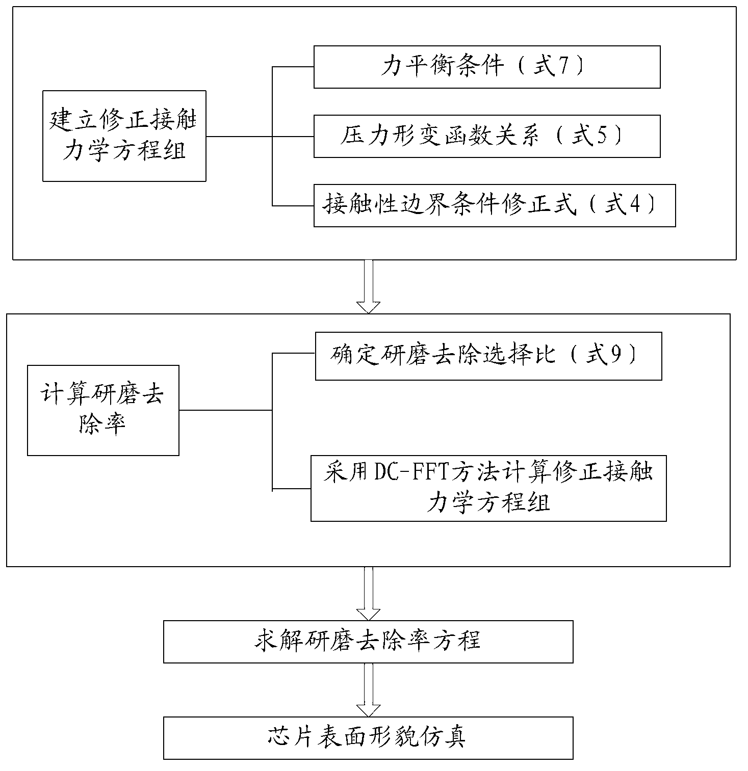
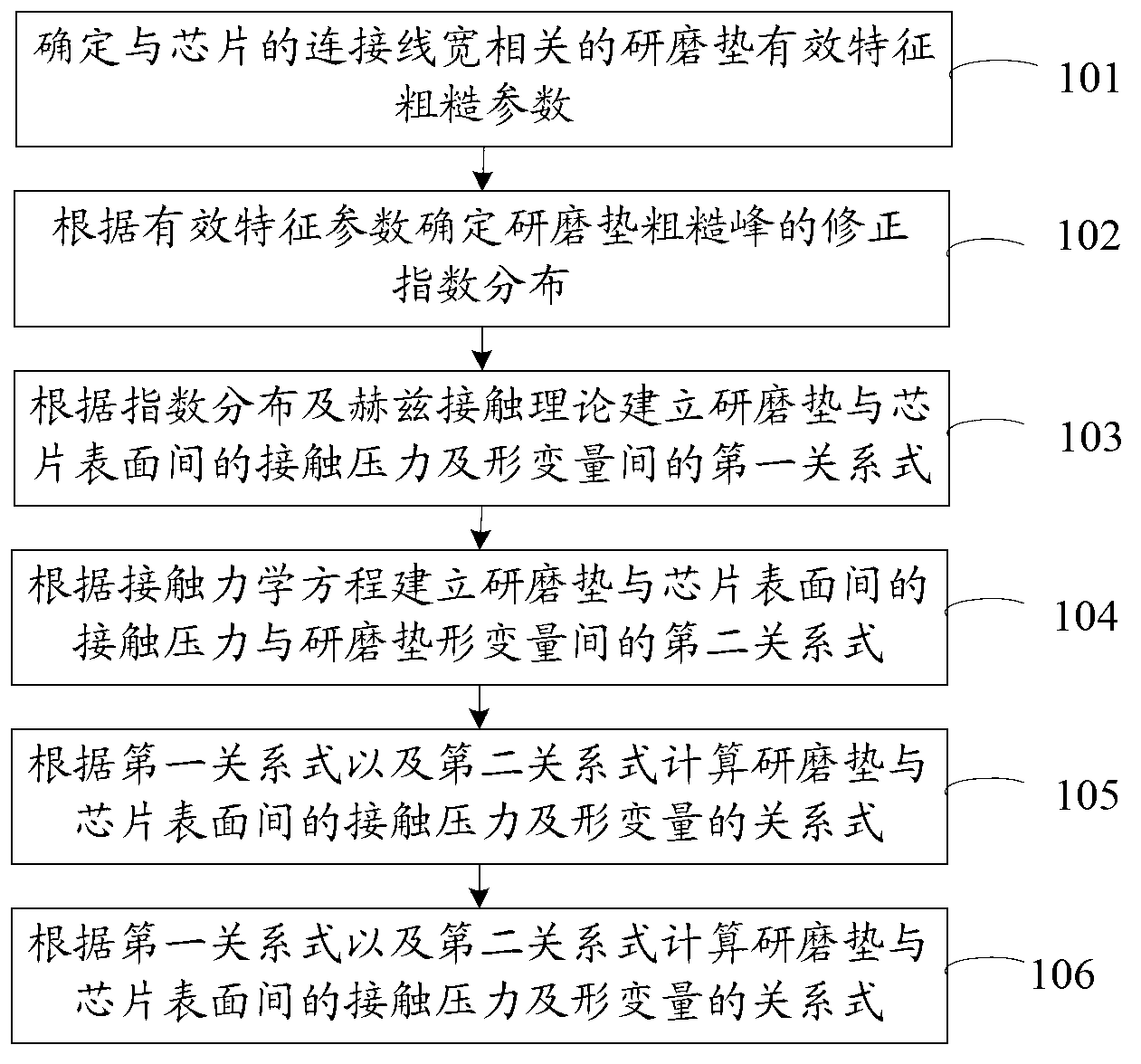
[0022] In order to make the above objects, features and advantages of the present invention more comprehensible, the embodiments of the present invention will be further described in detail below in conjunction with the accompanying drawings and specific implementation methods.

[0023] figure 1 It is a flow chart of the chip surface topography simulation method of the present invention.

[0024] Such as figure 1 As shown, the method includes the following steps:

[0025] Step 101: Determine the effective characteristic roughness parameters of the polishing pad related to the connection line width of the chip;

[0026] Step 102: Determine the modified exponential distribution of the roughness peak of the polishing pad according to the effective characteristic parameters;

[0027] Step 103: Establish a first relationship between the contact pressure between the polishing pad and the chip surface and the deformation of the polishing pad according to the exponential distributi...


PUM


Abstract

The invention discloses a simulation method and device for chip surface morphology, which are used for solving the problem that errors are bigger during simulation of GW model chip surface morphology. The method comprises the steps as follows: determining effective feature roughness parameter of a polishing pad relevant to a chip connecting linewidth; determining modified index distribution of a polishing pad rough peak according to the effective feature roughness parameter; establishing a first relation between the surface contact pressure of the polishing pad and the chip and polishing pad deformation according to the index distribution and the Hertz elastic theory; establishing a second relation between the polishing pad and the chip surface contact pressure and the polishing pad deformation according to a contact mechanics equation; calculating the relation between the polishing pad and the chip surface contact pressure and the polishing pad deformation according to the first relation and the second relation; and performing chip surface morphology simulation by using the relation of contact pressure and the deformation of the chip. The technical scheme provided by the invention avoids the wrong solution of the GW model in small linewidth CMP (chemical mechanical planarization) processing simulation, and improves the simulation and prediction accuracy of the GW model.

Description

technical field [0001] The invention relates to the field of chemical mechanical polishing, in particular to a method and device for simulating chip surface topography. Background technique [0002] Chemical Mechanical Planarization (CMP) was originally used to obtain high-quality glass surfaces. Since IBM first proposed the concept of integrated circuit "chemical mechanical polishing" in the early 1980s, CMP technology has gradually replaced traditional local polishing technology. It is widely used in various stages of integrated circuit manufacturing, and has become the only widely used technology to achieve ultra-fine processing of chip surface planarization in manufacturability design and integrated circuit process research and development. [0003] At present, the mainstream process technology of the 32 / 28 nanometer node is the high-k metal gate (High-k Metal Gate, HKMG) technology, which enables the development of semiconductor processes to continue with Moore's Law. ...

Claims


Application Information

Patent Timeline
Patent Type & Authority Applications(China)
IPC IPC(8): G06F17/50
Inventor 徐勤志陈岚
Owner INST OF MICROELECTRONICS CHINESE ACAD OF SCI
Why Eureka
Try Eureka