Supercharge Your Innovation With Domain-Expert AI Agents!

Image processing circuit, image processing method, liquid crystal display and electronic equipment

一种影像处理、液晶装置的技术,应用在静态指示器、仪器等方向,能够解决显示错反等问题,达到减小电位差、提高效果、抑制显示错反的效果

Active Publication Date: 2017-04-19
SEIKO EPSON CORP
View PDF11 Cites 0 Cited by
  • Summary
  • Abstract
  • Description
  • Claims
  • Application Information

AI Technical Summary

Problems solved by technology

[0005] However, in each frame, the larger the value of the time-integrated change in the transmittance of the liquid crystal element obtained by applying the correction voltage with respect to the application time, the easier it is for the user to perceive the display misalignment caused by the pixel to be corrected.
In the techniques disclosed in Patent Document 1 and Patent Document 2, it is considered that, in the pixel to be corrected, a constant correction voltage is applied to the liquid crystal element over the entire one frame period, so that display errors that are perceived by the user are likely to occur.

Method used


Image

  • Image processing circuit, image processing method, liquid crystal display and electronic equipment
  • Image processing circuit, image processing method, liquid crystal display and electronic equipment
  • Image processing circuit, image processing method, liquid crystal display and electronic equipment

Examples


no. 1 Embodiment approach >

[0065] First, a first embodiment of the present invention will be described.

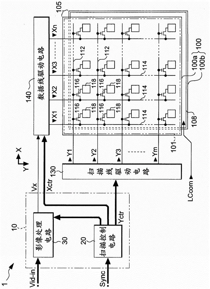
[0066] figure 1 It is a block diagram showing the overall configuration of the liquid crystal display 1 to which the video processing circuit according to this embodiment is applied.

[0067] Such as figure 1 As shown, the liquid crystal display 1 includes: a control circuit 10 , a liquid crystal panel 100 , a scanning line driving circuit 130 , and a data line driving circuit 140 . The video signal Vid-in is supplied from a host device to the control circuit 10 in synchronization with the synchronization signal Sync. The video signal Vid-in is digital data that specifies the gray level of each pixel of the liquid crystal panel 100, and is scanned according to a vertical scanning signal, a horizontal scanning signal, and a dot clock signal (all of which are not shown) included in the synchronous signal Sync. order to supply. In the present embodiment, the video signal Vid-in is supplied at a fre...

no. 2 Embodiment approach >

[0160] Next, a second embodiment of the present invention will be described. Also in this embodiment, description is made on the premise of the normal black mode. This point is also the same for the following embodiments unless otherwise specified. In the following description, the same configurations as those of the first embodiment are denoted by the same reference numerals, and detailed description thereof will be appropriately omitted. In the above-mentioned first embodiment, the image processing circuit 30 corrects the video signal only in the dark pixels adjacent to the risk boundary. An image signal of two or more consecutive dark pixels.

[0161] The video processing circuit 30 of this embodiment differs from the configuration of the first embodiment in the following two points: the content of discrimination by the discrimination unit 3042 is changed, and the pixel to be corrected by the correction unit 306 is changed.

[0162] The discrimination unit 3042 discrimin...

no. 3 Embodiment approach >

[0169] Next, a third embodiment of the present invention will be described.

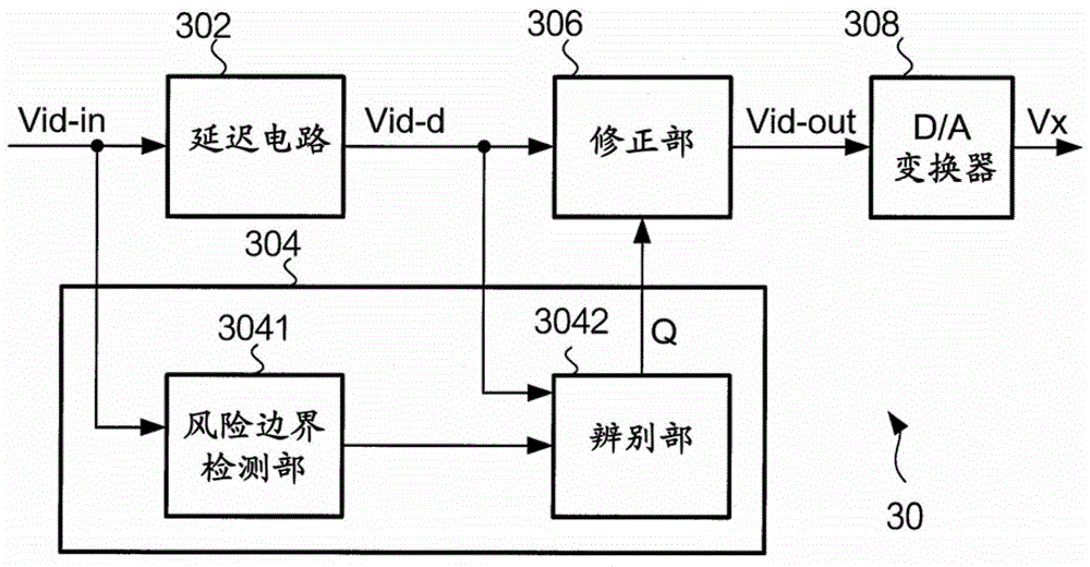
[0170] In this embodiment, the image processing circuit 30 corrects the image signal of the bright pixel adjacent to the risk boundary instead of the dark pixel adjacent to the risk boundary. In this embodiment, the correction unit 306 does not correct the video signal of dark pixels. In this case, a correction voltage lower than the applied voltage corresponding to the original gradation is applied during a part of one frame period (first period). Below, the corrected voltage for the first period is Figure 4 The "Vc2" indicated by , the corresponding corrected gray scale is "c2". The corrected grayscale c2 is a grayscale level belonging to the grayscale range d. Also, the corrected voltage for the second period is Figure 4 The "Vwt" indicated by , the corresponding corrected gray scale is "wt".

[0171] Even when bright pixels are used as correction target pixels, if the video processing circ...


PUM

PropertyMeasurementUnit
visible light transmittanceaaaaaaaaaa

Abstract

Changes in the transmittance of the liquid crystal element caused by the application of the correction voltage in each frame are suppressed, and the reverse tilt domain is reduced. It is characterized in that the image processing circuit (30) includes: a boundary detection unit, in the normal black mode, detects the first pixel whose applied voltage specified by the image signal (Vid-in) is lower than the first voltage and the applied voltage exceeds the above-mentioned The boundary of the second pixel of the second voltage with the first voltage higher than the first voltage; the correction unit corrects the video signal of the specified voltage applied to the liquid crystal element corresponding to the first pixel adjacent to the boundary detected by the boundary detection unit to: A correction voltage higher than the applied voltage is specified for a part of one frame period, and a video signal having a correction voltage lower than the applied voltage is specified for the rest of the one frame period.

Description

technical field [0001] The present invention relates to a technique for reducing defects in display of a liquid crystal panel. Background technique [0002] A liquid crystal panel has a configuration in which liquid crystal is sandwiched between pixel electrodes provided for each pixel and common electrodes provided in common to a plurality of pixels. In such a liquid crystal panel, liquid crystal misalignment (reverse tilt domain) occurs due to a transverse electric field generated by adjacent pixel electrodes, and this may cause display defects. Patent Document 1 and Patent Document 2 disclose techniques for suppressing the occurrence of display defects caused by poor alignment of liquid crystals. Patent Document 1 and Patent Document 2 disclose reducing the transverse electric field generated in a pixel to which a strong transverse electric field is applied and which tends to cause poor image quality due to the deposition direction of liquid crystal alignment (inorganic ...

Claims


Application Information

Patent Timeline
Patent Type & Authority Patents(China)
IPC IPC(8): G09G3/36
CPCG09G3/3614G09G3/3648G09G2320/0261G09G2340/0435G09G2360/16G09G3/3696
Inventor 北川拓保坂宏行
Owner SEIKO EPSON CORP
Features
  • R&D
  • Intellectual Property
  • Life Sciences
  • Materials
  • Tech Scout
  • Unparalleled Data Quality
  • Higher Quality Content
  • 60% Fewer Hallucinations
Learn More