Supercharge Your Innovation With Domain-Expert AI Agents!

Video processing circuit, video processing method, liquid crystal display device, and electronic apparatus

A technology for electronic equipment and liquid crystal devices, applied in static indicators, instruments, etc., can solve the problems of display error and reverse, and achieve the effect of reducing potential difference, suppressing display error and improving effect.

Active Publication Date: 2013-07-31
SEIKO EPSON CORP
View PDF11 Cites 2 Cited by
  • Summary
  • Abstract
  • Description
  • Claims
  • Application Information

AI Technical Summary

Problems solved by technology

[0005] However, in each frame, the larger the value of the time-integrated change in the transmittance of the liquid crystal element obtained by applying the correction voltage with respect to the application time, the easier it is for the user to perceive the display misalignment caused by the pixel to be corrected.
In the techniques disclosed in Patent Document 1 and Patent Document 2, it is considered that, in the pixel to be corrected, a constant correction voltage is applied to the liquid crystal element over the entire one frame period, so that display errors that are perceived by the user are likely to occur.

Method used


Image

  • Video processing circuit, video processing method, liquid crystal display device, and electronic apparatus
  • Video processing circuit, video processing method, liquid crystal display device, and electronic apparatus
  • Video processing circuit, video processing method, liquid crystal display device, and electronic apparatus

Examples


no. 1 Embodiment approach >

[0065] First, a first embodiment of the present invention will be described.

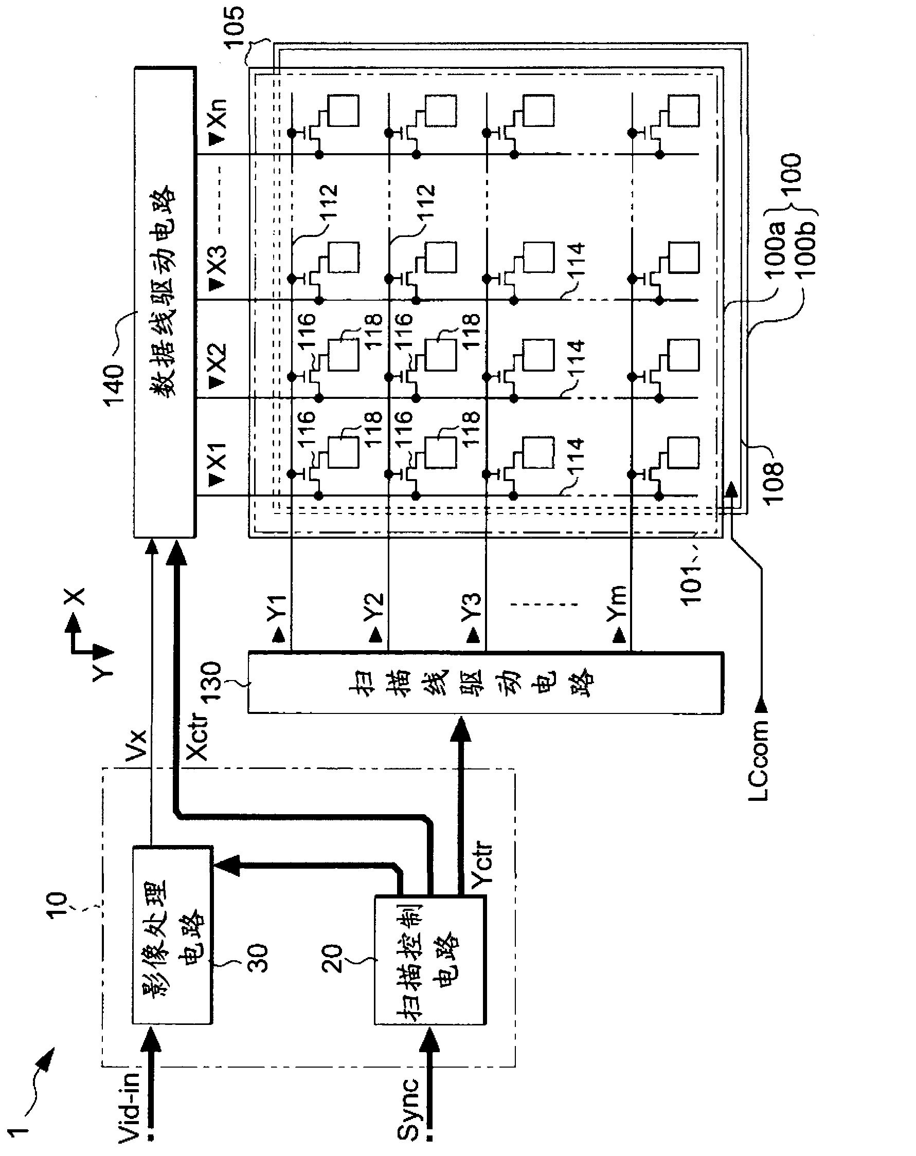
[0066] figure 1 It is a block diagram showing the overall configuration of the liquid crystal display 1 to which the video processing circuit according to this embodiment is applied.

[0067] Such as figure 1 As shown, the liquid crystal display 1 includes: a control circuit 10 , a liquid crystal panel 100 , a scanning line driving circuit 130 , and a data line driving circuit 140 . The video signal Vid-in is supplied from a host device to the control circuit 10 in synchronization with the synchronization signal Sync. The video signal Vid-in is digital data that specifies the gray level of each pixel of the liquid crystal panel 100, and is scanned according to a vertical scanning signal, a horizontal scanning signal, and a dot clock signal (all of which are not shown) included in the synchronous signal Sync. order to supply. In the present embodiment, the video signal Vid-in is supplied at a fre...

no. 2 Embodiment approach >

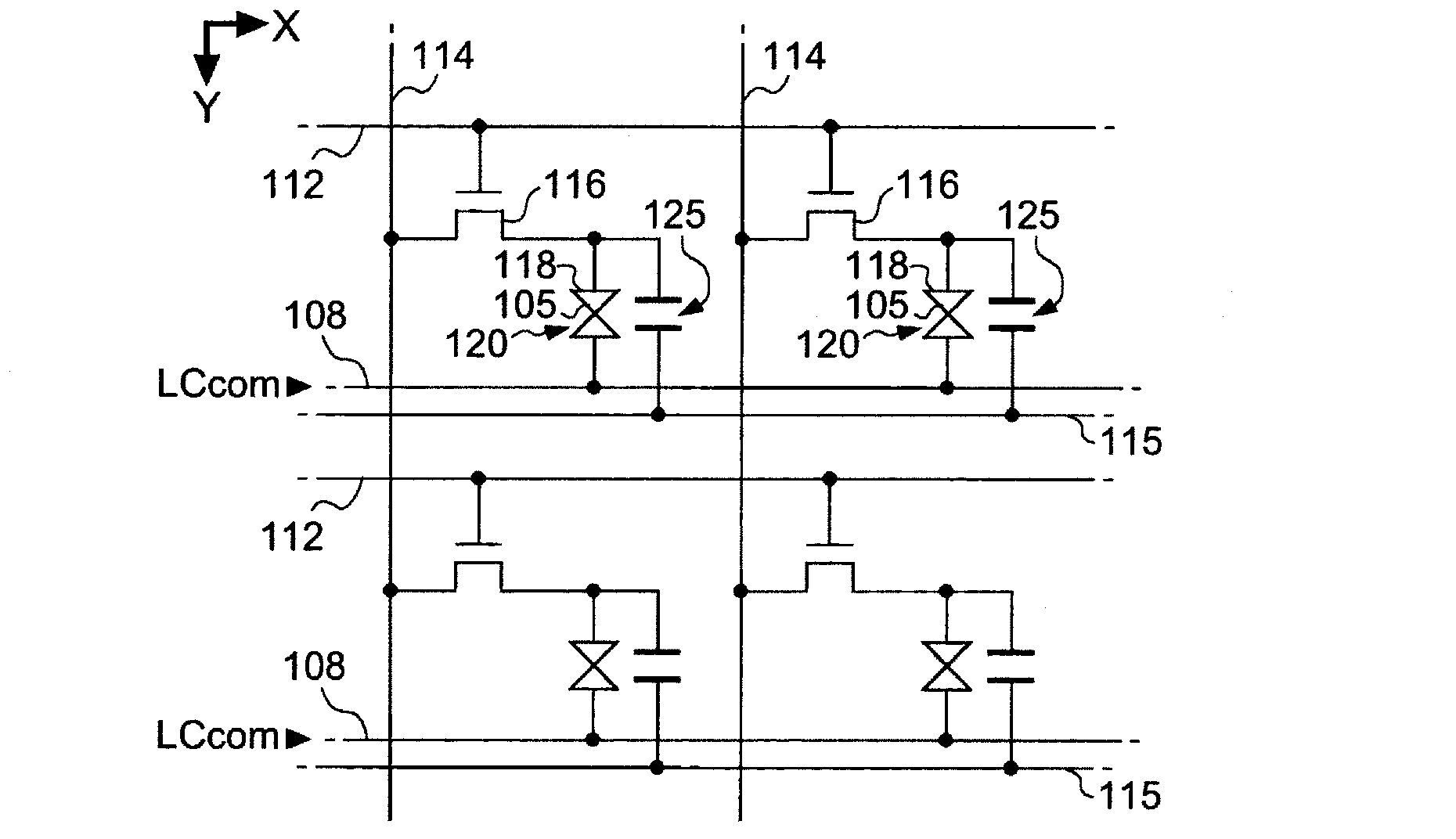
[0160] Next, a second embodiment of the present invention will be described. Also in this embodiment, description is made on the premise of the normal black mode. This point is also the same for the following embodiments unless otherwise specified. In the following description, the same configurations as those of the first embodiment are denoted by the same reference numerals, and detailed description thereof will be appropriately omitted. In the above-mentioned first embodiment, the image processing circuit 30 corrects the video signal only in the dark pixels adjacent to the risk boundary. An image signal of two or more consecutive dark pixels.

[0161] The video processing circuit 30 of this embodiment differs from the configuration of the first embodiment in the following two points: the content of discrimination by the discrimination unit 3042 is changed, and the pixel to be corrected by the correction unit 306 is changed.

[0162] The discrimination unit 3042 discrimin...

no. 3 Embodiment approach >

[0169] Next, a third embodiment of the present invention will be described.

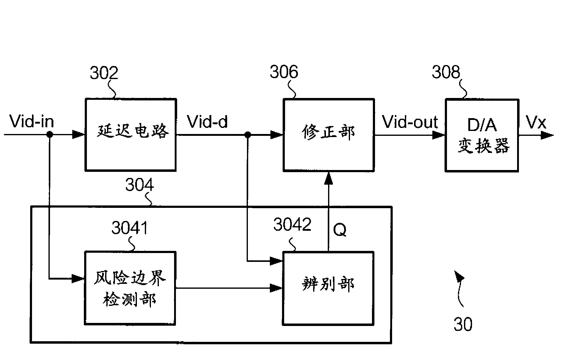
[0170] In this embodiment, the image processing circuit 30 corrects the image signal of the bright pixel adjacent to the risk boundary instead of the dark pixel adjacent to the risk boundary. In this embodiment, the correction unit 306 does not correct the video signal of dark pixels. In this case, a correction voltage lower than the applied voltage corresponding to the original gradation is applied during a part of one frame period (first period). Below, the corrected voltage for the first period is Figure 4 The "Vc2" indicated by , the corresponding corrected gray scale is "c2". The corrected grayscale c2 is a grayscale level belonging to the grayscale range d. Also, the corrected voltage for the second period is Figure 4 The "Vwt" indicated by , the corresponding corrected grayscale is "wt".

[0171] Even when bright pixels are used as correction target pixels, if the video processing circu...


PUM


Abstract

A video processing circuit includes a boundary detection unit which detects a boundary between a first pixel in which an application voltage which is designated by a video signal Vid-in is lower than a first voltage and a second pixel which exceeds a second voltage in which the application voltage is higher than the first voltage in a normally black mode; and a correction unit which corrects a video signal in which an application voltage to a liquid crystal element corresponding to the first pixel which comes into contact with a boundary detected by the boundary detection unit is designated to be a video signal in which a correction voltage which is higher than the application voltage is designated in a part of period of one frame period, and a correction voltage which is lower than the application voltage is designated in other periods of the one frame period.

Description

technical field [0001] The present invention relates to a technique for reducing defects in display of a liquid crystal panel. Background technique [0002] A liquid crystal panel has a configuration in which liquid crystal is sandwiched between pixel electrodes provided for each pixel and common electrodes provided in common to a plurality of pixels. In such a liquid crystal panel, liquid crystal misalignment (reverse tilt domain) occurs due to a transverse electric field generated by adjacent pixel electrodes, and this may cause display defects. Patent Document 1 and Patent Document 2 disclose techniques for suppressing the occurrence of display defects caused by poor alignment of liquid crystals. Patent Document 1 and Patent Document 2 disclose reducing the transverse electric field generated in a pixel to which a strong transverse electric field is applied and which tends to cause poor image quality due to the deposition direction of liquid crystal alignment (inorganic ...

Claims


Application Information

Patent Timeline
Patent Type & Authority Applications(China)
IPC IPC(8): G09G3/36
CPCG09G2360/16G09G3/3614G09G2340/0435G09G3/3696G09G3/3648G09G2320/0261
Inventor 北川拓保坂宏行
Owner SEIKO EPSON CORP
Features
  • R&D
  • Intellectual Property
  • Life Sciences
  • Materials
  • Tech Scout
  • Unparalleled Data Quality
  • Higher Quality Content
  • 60% Fewer Hallucinations
Learn More