CLB-bus-based NorFLASH memory interface chip with high utilization ratio

A storage interface and utilization technology, applied in the field of NorFLASH storage interface chips, can solve the problems of multiple CPU resource operation steps, many port control signals, cumbersome and other problems, and achieve simple read and write operation steps, strong versatility, and improved utilization. Effect

Active Publication Date: 2013-08-07
苏州国芯科技股份有限公司
View PDF2 Cites 9 Cited by
  • Summary
  • Abstract
  • Description
  • Claims
  • Application Information

AI Technical Summary

Problems solved by technology

[0003] The object of the present invention is to provide a high-utilization NorFLASH storage interface chip based on the CLB bus, which can improve the utilization of NorFLASH to a greater extent; Run the code directly on the chip, with excellent stability and high transmission rate, which is very suitable for embedded systems. As the advantage of NorFLASH ROM, it solves the problem that there are many control signals on the NorFLASH port, and the implementation of direct register control will consume a lot of CPU resources and operation steps Complicated problems; simple operation, consumes less CPU resources, and facilitates software development

Method used


Image

  • CLB-bus-based NorFLASH memory interface chip with high utilization ratio
  • CLB-bus-based NorFLASH memory interface chip with high utilization ratio
  • CLB-bus-based NorFLASH memory interface chip with high utilization ratio

Examples


Embodiment

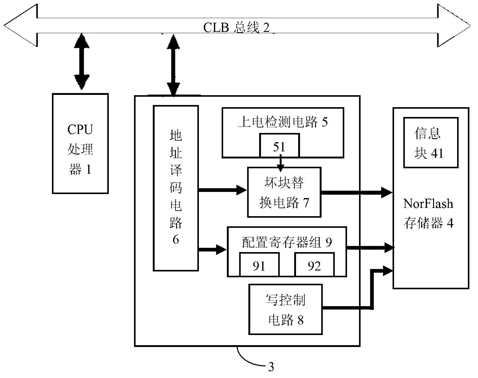
[0029] Embodiment: a kind of NorFLASH storage interface chip with high utilization rate based on CLB bus, comprising CPU processor 1, CLB bus 2, NorFlash interface unit 3, NorFlash memory 4, described NorFlash memory 4 passes CLB bus 2 via NorFlash interface unit 3 Communicate with CPU processor 1; Described NorFlash interface unit 3 further comprises power-on detection circuit 5, address decoding circuit 6, bad block replacement circuit 7, write control circuit 8 and configuration register group 9 and are used to display last operating state The status register group 10;

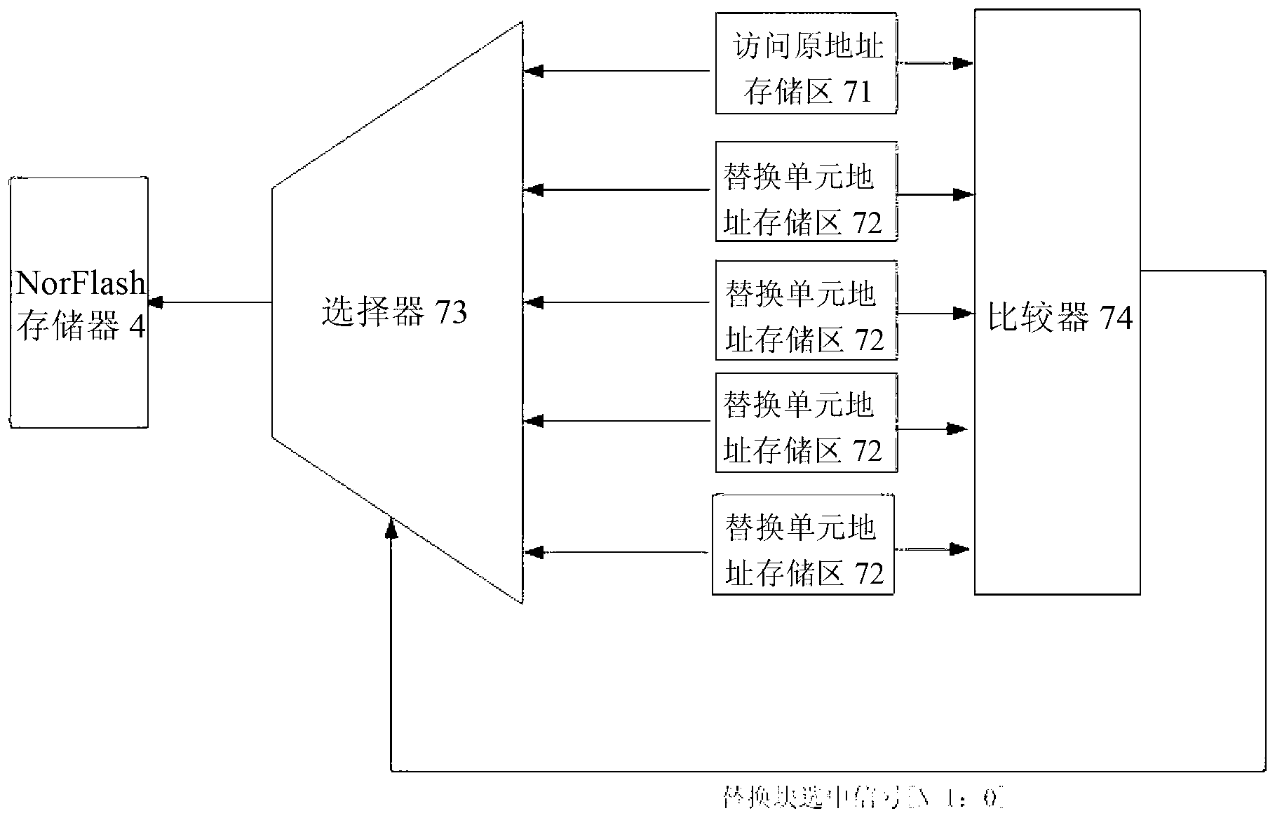
[0030] There is an information block 41 in the described NorFlash memory 4, and this information block 41 records the address of the bad block unit in the NorFlash memory 4, the address of the number, the replacement unit and the replacement unit to replace the bad block function enabling bit information, and this enabling bit is effective There is a bad block in the identification NorFlash memory 4, and th...


PUM


Abstract

The invention provides a CLB-bus-based NorFLASH memory interface chip with high utilization ratio. The memory interface chip comprises a CPU processor, a CLB bus, a NorFlash interface unit and a NorFlash memory, wherein the NorFlash memory communicates with the CPU processor through the NorFlash interface unit by the CLB bus; the NorFlash interface unit further comprises a power-on detection circuit, an address decoding circuit, a bad block replacement circuit and a writing control circuit, as well as a configuration register set and a state register set; an information block is arranged in the NorFlash memory and records the addresses and the number of bad blocks in the NorFlash memory and the bad block replacement function enabling information of a replacement unit; a bad block register used for storing information from the information block is arranged in the power-on detection circuit; and the bad block replacement circuit is used for re-mapping the addresses of the bad blocks. The NorFLASH memory interface chip improves the NorFLASH utilization ratio to a greater extent.

Description

technical field [0001] The invention relates to a NorFLASH storage interface chip, in particular to a high-utilization NorFLASH storage interface chip based on a CLB bus. Background technique [0002] NorFLASH can run code directly on the chip, with excellent stability and high transmission rate, which is very suitable for embedded systems as NorFLASH ROM. At present, NorFLASH has been widely used in SOC chips (System on Chip, called system-on-chip, also known as system-on-chip). Appropriate interface design is crucial to the application of NorFLASH on SOC chips. When reading and writing NorFLASH operations, it is necessary to control many control signals on it. If the NorFLASH control signals are directly implemented by register control, it will consume a lot of CPU resources, and the operation steps are cumbersome. It takes a lot of software resources to operate and replace the steps, and the software maintenance is more complicated. Therefore, how to provide a NorFLASH...

Claims


Application Information

Patent Timeline
Patent Type & Authority Applications(China)
IPC IPC(8): G06F12/02
Inventor 郑茳肖佐楠匡启和林雄鑫周秀梅
Owner 苏州国芯科技股份有限公司
Why Eureka
Try Eureka