Linear defect repairing method of liquid crystal display array substrate

A liquid crystal array and repair method technology, applied in nonlinear optics, instruments, optics, etc., can solve the problems of foreign matter, irreparable, affecting product yield, etc.

Active Publication Date: 2013-08-21
NANJING CEC PANDA LCD TECH
View PDF5 Cites 15 Cited by
  • Summary
  • Abstract
  • Description
  • Claims
  • Application Information

AI Technical Summary

Problems solved by technology

[0003] In the process of actually fabricating the array substrate, such as image 3 As shown, the short circuit between the scanning line (gate line) 12 and the common electrode line (Com line), or the occurrence rate of the open circuit defect of the scanning line (gate line) is relatively hi

Method used


Image

  • Linear defect repairing method of liquid crystal display array substrate
  • Linear defect repairing method of liquid crystal display array substrate
  • Linear defect repairing method of liquid crystal display array substrate

Examples


Example Embodiment

[0023] In the following, the present invention will be further clarified with reference to the accompanying drawings and specific embodiments. It should be understood that these embodiments are only used to illustrate the present invention and not to limit the scope of the present invention. After reading the present invention, those skilled in the art have Modifications in equivalent forms fall within the scope defined by the appended claims of this application.
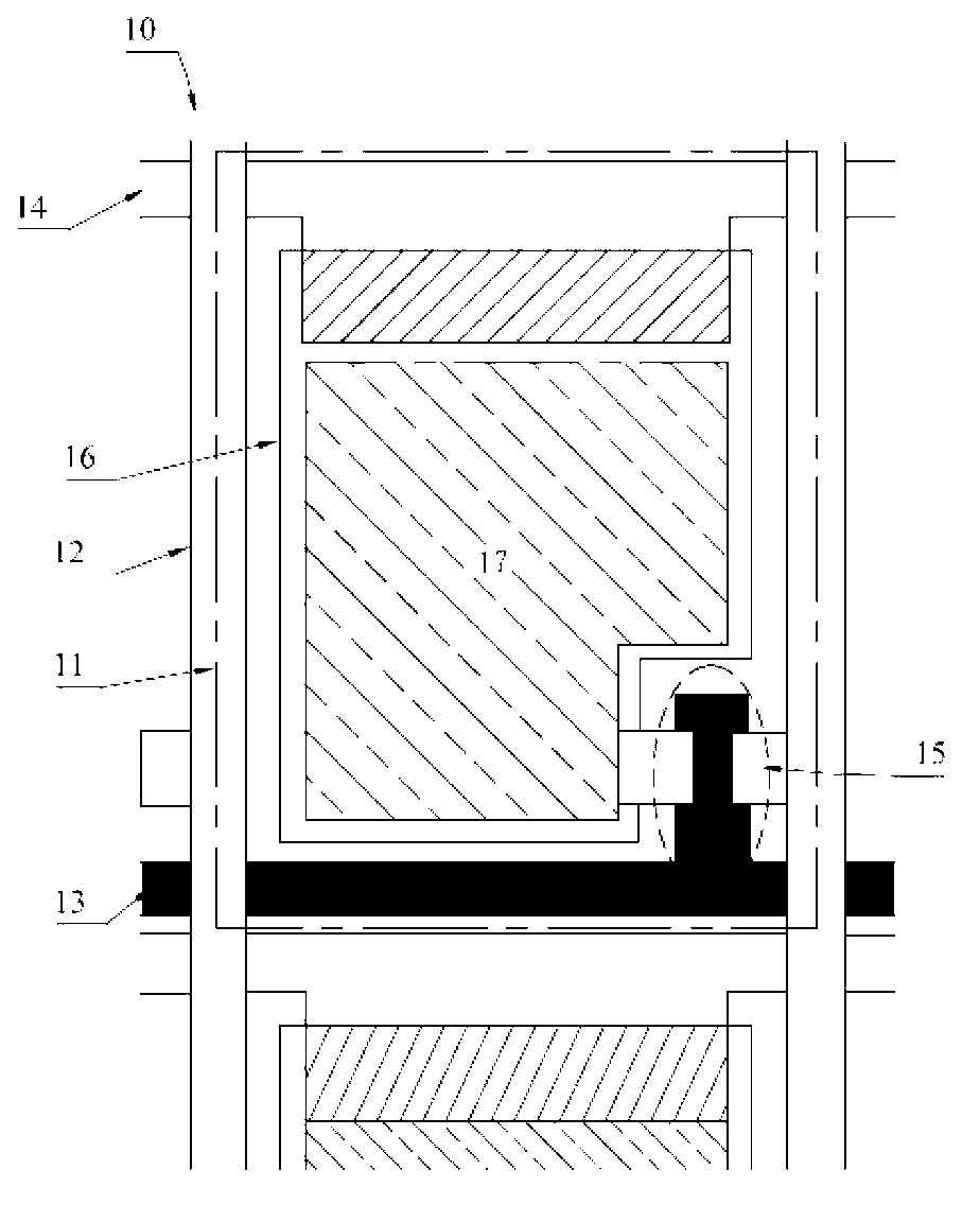
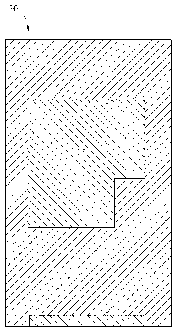
[0024] The present invention protects a method for repairing line defects of liquid crystal display array substrates, such as image 3 Shown is a schematic structural diagram of a liquid crystal display array substrate of the present invention, which includes: criss-crossed scan lines 10 and data lines 20, common electrode lines 30 in the same layer as scan lines 10, pixel electrodes 40, thin film transistors 50, The line 10 and the data line 20 are separated by a gate insulating layer (not shown), and the data line 20 ...


PUM


Abstract

The invention provides a linear defect repairing method of a liquid crystal display array substrate. A liquid crystal array substrate comprises scanning lines, data lines staggered with scanning lines, common electrode lines parallel with the scanning lines and a plurality of pixel units limited by the scanning lines and the data lines in a crossed manner. Each pixel unit comprises a thin film transistor and a pixel electrode. Each thin film transistor comprises a grid formed along with the scanning lines, a source connected with the data lines and a drain connected with the pixel electrodes. Common electrode lines of adjacent pixel units are connected through a connecting line. When scanning line breakage or scanning line and common electrode short circuit of the array substrate occurs, a part of dependent common electrode line areas can be separated or scanning lines can be isolated, then a laser repairing machine can be used to communicate two ends of drains of adjacent pixel units with scanning lines and common electrode lines respectively so as to complete repairing. Though a few pixel units lose, repairing success rate can be increased, and cost can be saved.

Description

technical field [0001] The invention relates to a method for repairing line defects of a liquid crystal display array substrate. Background technique [0002] Such as figure 1 with figure 2 Shown is a schematic plan view of an existing common liquid crystal display device. The existing liquid crystal display device includes an array substrate 10 and a color filter substrate 20 facing each other, and a liquid crystal interposed between the array substrate 10 and the color filter substrate 20 (not shown in the figure). ), each pixel unit 11 of the array substrate 10 includes: criss-cross data lines 12 and scan lines 13, storage capacitor lines 14 (abbreviated as COM lines), transistors 15, and pixel electrodes 16. The pixel electrodes 16 have effective light-transmitting Area 17, the pixel aperture ratio refers to the light passing through the array unit 11 after excluding the wiring areas such as the data line 12, the scanning line 13, the storage capacitor line 14 (referr...

Claims


Application Information

Patent Timeline
IPC IPC(8): G02F1/13G02F1/1362G02F1/1368
Inventor 杭传静
Owner NANJING CEC PANDA LCD TECH
Why Eureka
Try Eureka