
Self-repair device

a self-repair and memory device technology, applied in the direction of static storage, instruments, etc., can solve the problems of inefficient discarding entire semiconductor memory devices, failures occurring probabilistically in only a small number of memory cells, and mis-operation of corresponding semiconductor memory devices, so as to reduce the layout area, reduce the number of fuse registers, and increase the repair success rate

Active Publication Date: 2015-11-17
SK HYNIX INC
View PDF23 Cites 4 Cited by
  • Summary
  • Abstract
  • Description
  • Claims
  • Application Information

AI Technical Summary

Benefits of technology

This patent describes a device that can repair failed parts of a semiconductor device using a redundancy of information. The device can determine if the fail is related to a specific part (a "cracked row" or "short column") and select the appropriate part to repair it, increasing the success rate. Additionally, the device can reduce the number of fuse registers needed by only loading non-used fuse sets and using information from failed parts. This decrease in the number of fuse registers and layout area can lead to more efficient repair processes.

Problems solved by technology

If a fail occurs in even any one among memory cells, a corresponding semiconductor memory device mis-operates.
However, recently, as processing technologies for manufacturing semiconductor memory devices have been further developed, fails occur probabilistically in only a small number of memory cells.
When considering the yield of a product, it is inefficient to discard entire semiconductor memory devices as failed products due to a small number of fails.
As a net die increases and it is complicated to realize a column redundancy control circuit, an existing self-repair device is performs only a row repair operation.
According to this fact, since it is impossible to repair a column-related fail, a repair success rate becomes poor.

Method used


Image

  • Self-repair device
  • Self-repair device
  • Self-repair device

Examples


Embodiment Construction

[0029]Hereinafter, a self-repair device according to the invention will be described below with reference to the accompanying drawings through various embodiments.

[0030]As the sizes of respective elements constituting a is semiconductor integrated circuit device gradually decrease and the number of elements included in one semiconductor chip gradually increases, the level of defect density rises. The rise in defect density is a direct factor that lowers the yield of a semiconductor device. If the defect density markedly increases, a wafer on which semiconductor devices are formed should be discarded.

[0031]In order to decrease the defect density, a redundancy circuit which replaces defective cells with redundancy cells has been suggested. In the case of a semiconductor memory device, a redundancy circuit (or a fuse circuit) may be used for each of a row-related line (for example, a word line) and a column-related line (for example, a bit line).

[0032]Such a redundancy circuit includes...


PUM


Abstract

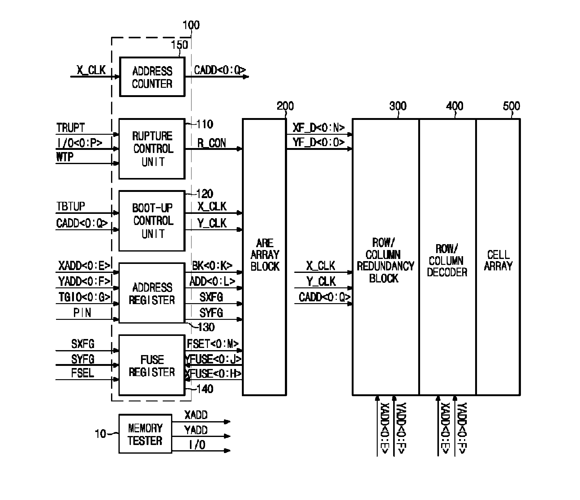
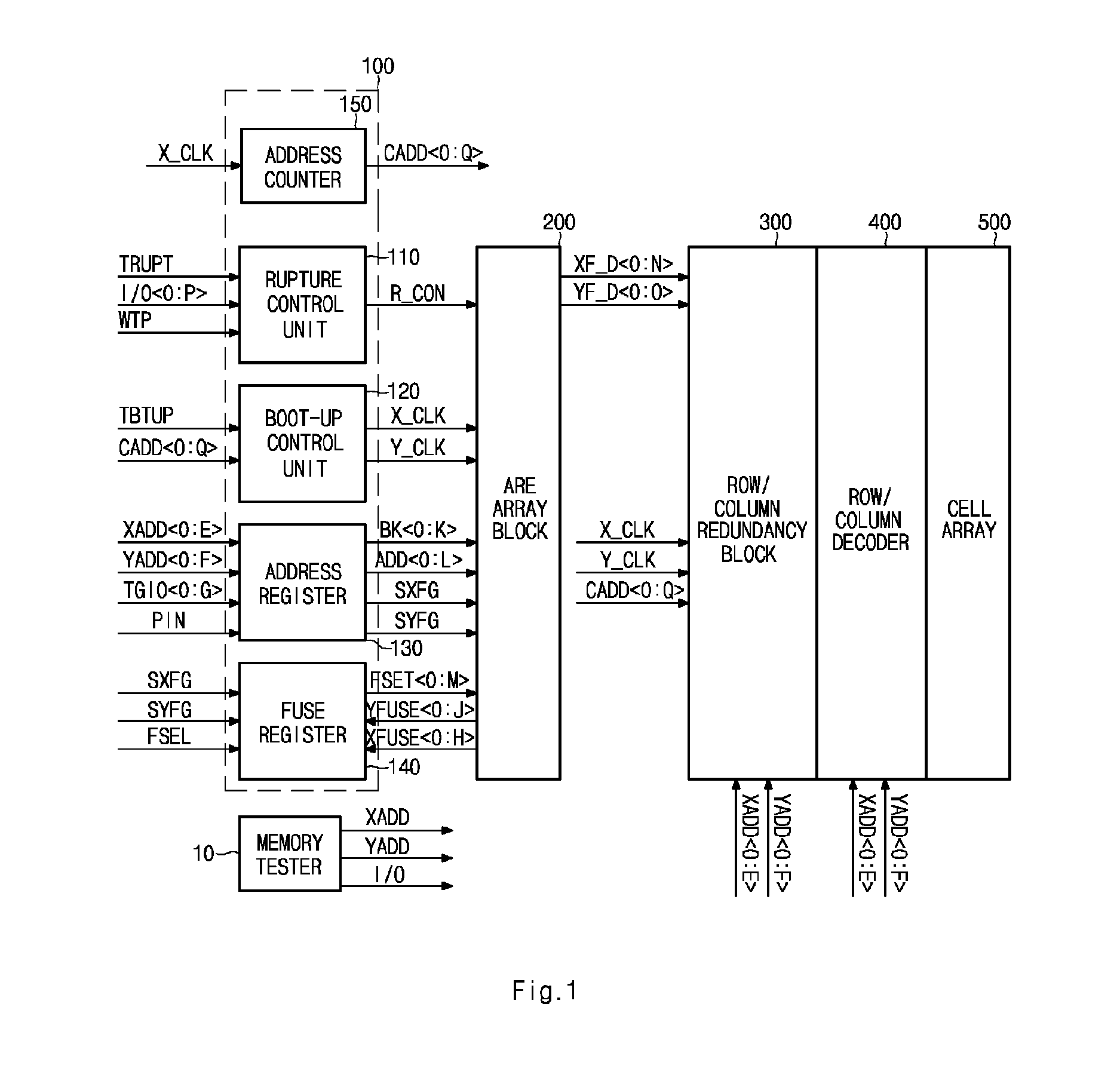
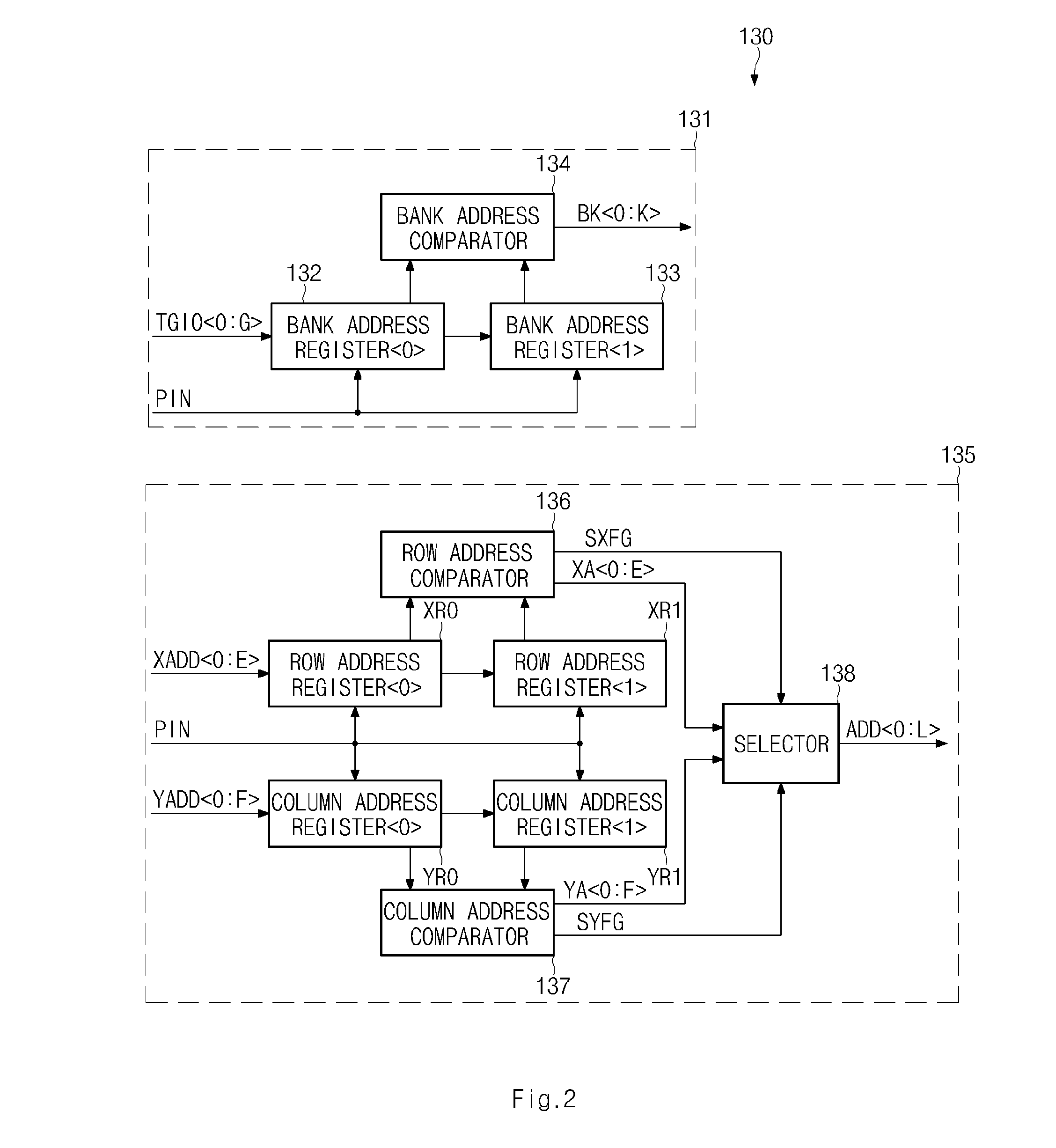
A self-repair device includes an ARE (array rupture electrical fuse) array block configured to store fail addresses; an ARE control block configured to control a repair operation of fuse sets according to the fail addresses, compare a plurality of the fail addresses, and determine a failed state; and a redundancy block configured to store fuse data of the fail addresses, compare an input address with the fail addresses, and control row and column redundancy operations.

Description

CROSS-REFERENCES TO RELATED APPLICATION[0001]The present application claims priority under 35 U.S.C. §119(a) to Korean application number 10-2013-109649, filed on Sep. 12, 2013, in the Korean Intellectual Property Office, which is incorporated herein by reference in its entirety.BACKGROUND[0002]1. Technical Field[0003]Various embodiments relate to a self-repair device, and more particularly, to a technology for improving the repair efficiency and reducing the area of a semiconductor device including a fuse array.[0004]2. Description of Related Art[0005]In general, a semiconductor memory device includes a is number of memory cells. As processing technologies have been developed and thus the degree of integration is augmented, the number of memory cells gradually increases. If a fail occurs in even any one among memory cells, a corresponding semiconductor memory device mis-operates. Therefore, since the semiconductor memory device including a failed cell cannot perform a desired opera...

Claims


Application Information

Patent Timeline
Patent Type & Authority Patents(United States)
IPC IPC(8): G11C29/00
CPCG11C29/787G11C29/808G11C29/04G11C29/12
Inventor SHIM, YOUNG BO
Owner SK HYNIX INC
Learn More