Imaging apparatus and image sensor array

A technology of image sensors and camera devices, applied in image communication, radiation control devices, instruments, etc., can solve problems such as complex volume, device complexity, and device compactness

Inactive Publication Date: 2013-08-21
SONY CORP
View PDF4 Cites 30 Cited by
  • Summary
  • Abstract
  • Description
  • Claims
  • Application Information

AI Technical Summary

Problems solved by technology

Therefore, light loss occurs in the lens system, among other problems such as difficulty in making the device more compact
The technique disclosed in Unexamined Japanese Patent Application Publication No. 2004-309868 requires the use of a combination of two pairs of lenses and polarizing filters, making it difficult to avoid a more complex and bulky device
Furthermore, using such a camera device to capture normal 2D images instead of just stereoscopic images creates additional device complexity and is not practical

Method used


Image

  • Imaging apparatus and image sensor array
  • Imaging apparatus and image sensor array
  • Imaging apparatus and image sensor array

Examples


example 2

[0049] 3. Example 2 (camera device and image sensor array according to the second mode of the present invention)

example 3

[0050] 4. Example 3 (camera device and image sensor array according to the third mode of the present invention)

[0051] 5. Example 4 (camera device and image sensor array according to the fourth mode of the present invention)

[0052] 6. Example 5 (camera device and image sensor array according to the fifth mode of the present invention)

example 6

[0053] 7. Example 6 (camera device and image sensor array according to the sixth mode of the present invention)

[0054] 8. Example 7 (Modifications of Example 4 to Example 6) and others

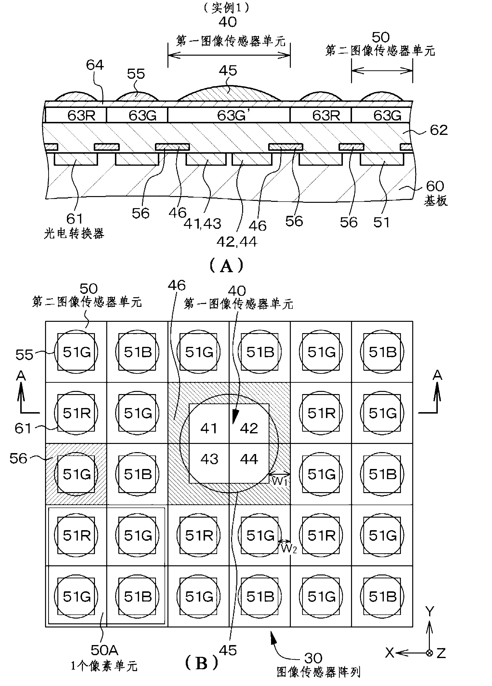
[0055] [Overall Explanation of Imaging Devices and Image Sensor Arrays According to the First Mode to the Sixth Mode of the Present Invention]

[0056] In the following description, in some cases, the first image sensor unit in the imaging device and the image sensor array according to the first mode to the third mode of the present invention and the imaging device and the imaging device according to the fourth mode to the sixth mode of the present invention The image sensor cells in the image sensor array may be collectively referred to as "(first) image sensor cells". Similarly, in some cases, the first microlens in the imaging device and image sensor array according to the first mode to the third mode of the present invention is the same as that in the imaging device and image sensor arr...


PUM


Abstract

The invention aims to provide an imaging apparatus for imaging an object to a stereo image and possessing a simple structure as well as an image sensor array used for the imaging apparatus. The imaging apparatus includes an imaging lens, and an image sensor array of first and second image sensor units, wherein a single first image sensor unit includes a single first microlens and a plurality of image sensors, a single second image sensor unit includes a single second microlens and a single image sensor, light passing through the imaging lens and reaching each first image sensor unit passes through the first microlens and forms an image on the image sensors constituting the first image sensor unit, light passing through the imaging lens and reaching each second image sensor unit passes through the second microlens and forms an image on the image sensor constituting the second image sensor unit, an inter-unit light shielding layer is formed between the image sensor units, and a light shielding layer is not formed between the image sensor units constituting the first image sensor unit.

Description

technical field [0001] The present invention relates to an imaging device and an image sensor array, more specifically, to an imaging device capable of imaging an object into a stereoscopic image and an image sensor array used in the imaging device. Background technique [0002] In the past, various imaging devices have been proposed and developed. In addition, there have been proposed imaging devices that perform given image processing on imaging signals obtained by imaging and output the resultant results, such as imaging devices that image a subject as a stereoscopic image. For example, International Publication No. 06 / 039486 proposes an imaging device using a technique called light field photography. The imaging device includes an imaging lens, a microlens array (light field lens), a photosensitive element and an image processor. The imaging signal obtained from the photosensitive element contains information on the intensity of light at the photosensitive surface of t...

Claims


Application Information

Patent Timeline
Patent Type & Authority Applications(China)
IPC IPC(8): H04N13/02H04N5/232G02B27/22H01L27/146H04N13/239
CPCH04N13/218H04N13/239H04N13/257H01L27/14621H01L27/14627H01L27/14623H04N25/702H04N25/134H04N25/70
Inventor 山崎知洋
Owner SONY CORP
Why Eureka
Try Eureka