
IC device having electromigration resistant feed line structures

A device and active circuit technology, applied in the field of IC devices with anti-electromigration feeder structure, can solve problems such as low efficiency and increased processing steps

Active Publication Date: 2013-08-21
TEXAS INSTR INC
View PDF4 Cites 0 Cited by
  • Summary
  • Abstract
  • Description
  • Claims
  • Application Information

AI Technical Summary

Problems solved by technology

This known solution increases the processing steps and is only inefficient since it is not able to induce a uniform current density for typical column sizes

Method used


Image

  • IC device having electromigration resistant feed line structures
  • IC device having electromigration resistant feed line structures
  • IC device having electromigration resistant feed line structures

Examples


Embodiment Construction

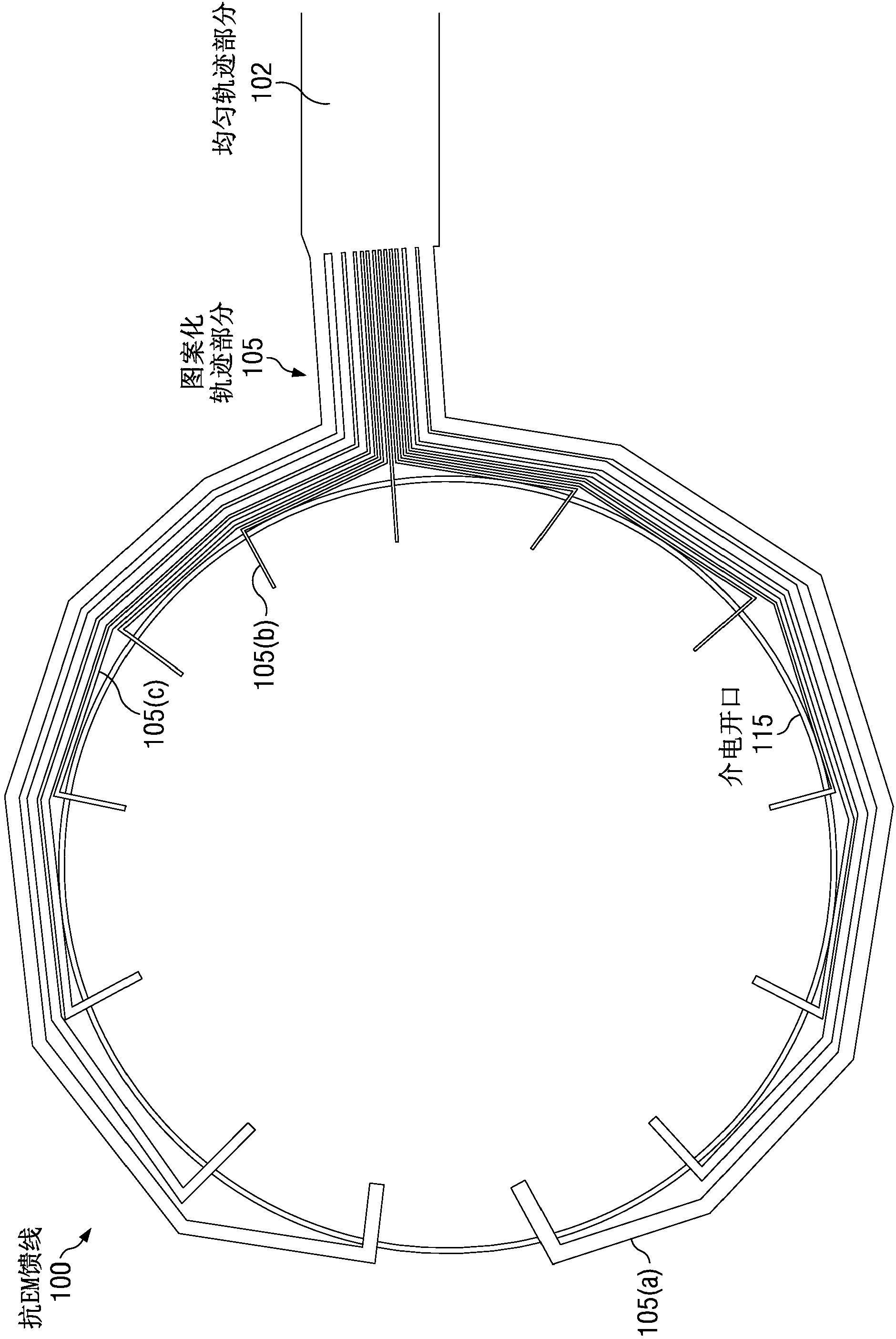
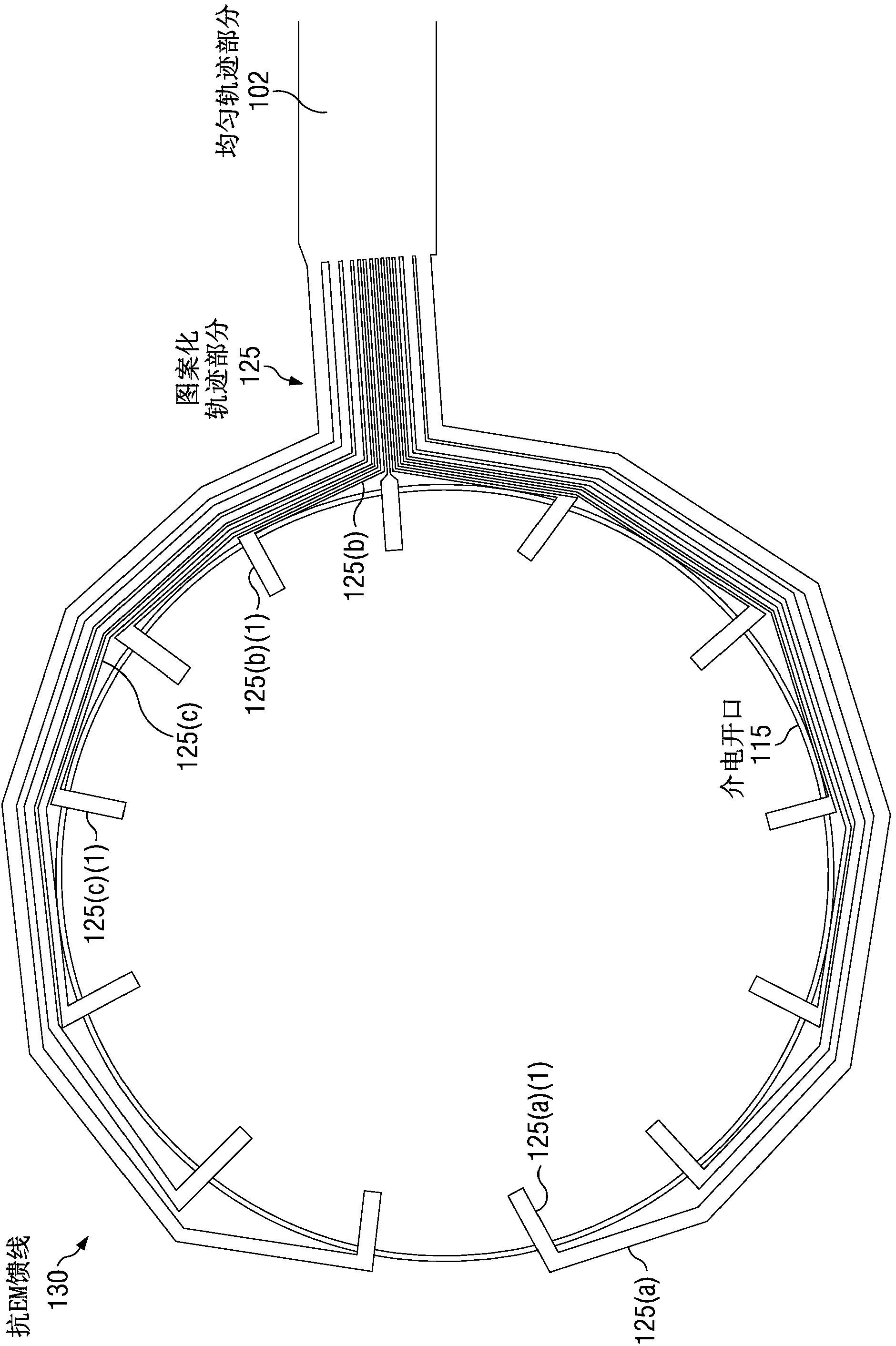
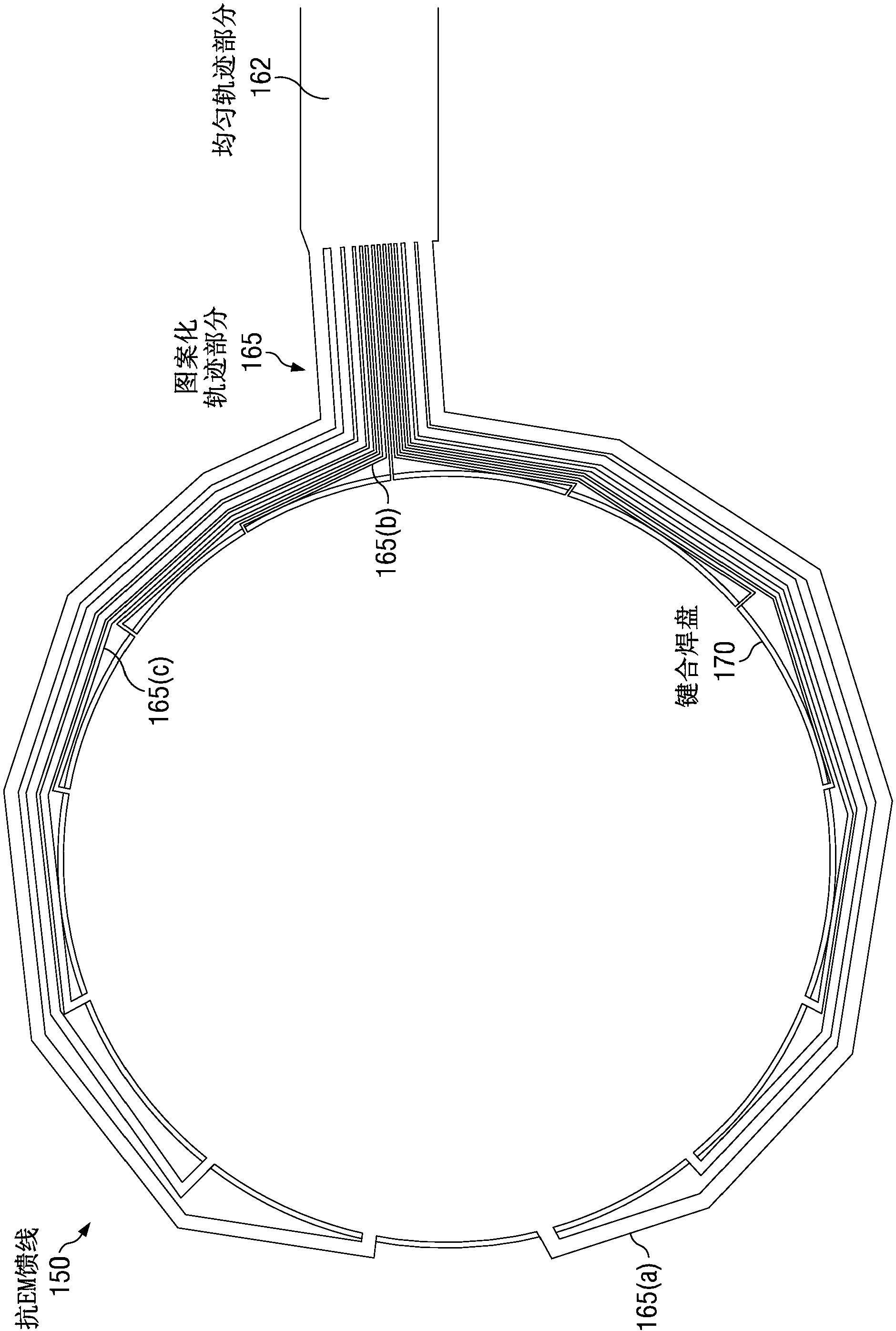
[0022] Figure 1A An example EM resistant feedline structure 100 is shown providing an edge feed with at least three sub-traces providing substantially equal sub-trace currents distributed substantially equally around the circumference of the dielectric opening 115 under the bond according to an example embodiment. although Figure 1A One larger dielectric opening 115 is shown in , but disclosed embodiments may instead include smaller dielectric openings or both larger and smaller dielectric openings under later formed bonds. . Bonds are generally described herein as solder bumps. However, the bond may also contain through-substrate vias (TSVs), pillars (e.g., copper pillars), studs (e.g., gold studs), or organic bonds with multiple metal particles. material.

[0023] The EM resistant feedline structure 100 comprises a uniform (eg, conventional) trace portion 102 coupled to a patterned trace portion 105 comprising at least three electrically parallel and distributed traces 1...


PUM


Abstract

An integrated circuit (IC) device (400) includes an electromigration (EM) resistant feed line (401). The IC device includes a substrate (405) including active circuitry (409). A back end of the line (BEOL) metallization stack (420) includes an interconnect metal layer (412) that is coupled to a bond pad (419) by the EM resistant feed line. A bonding feature (435) is on the bond pad. The EM resistant feed line (401) includes a uniform portion (402) and patterned trace portion (405) that extends to the bond pad which includes at least three sub-traces that are electrically in parallel. The sub-traces are sized so that a number of squares associated with each of the sub-traces is within a range of a mean number of squares for the sub-traces plus or minus twenty percent or a current density provided to the bonding feature through each sub- trace is within a range of a mean current density provided to the bonding feature plus or minus twenty percent.

Description

technical field [0001] The disclosed embodiments relate to integrated circuits (ICs) including feedline structures that enhance electromigration (EM) performance. Background technique [0002] An integrated circuit generally includes a substrate, active circuitry formed on top of the substrate, and a back-end-of-line (BEOL) structure including spacer metal wiring layers and an interlayer dielectric (ILD) over the active circuitry. The metal wiring layer contains various interconnect lines that provide electrical connections between active circuitry and external connections. Solder bumps (or solder balls) are typically used to provide a connection between the last (e.g., top) metal wiring level of a semiconductor device and another device, such as forming an active circuit or a node in cases where the interconnect acts as a passive role whereas solder bumps are only part of the via (eg for stacked die / package). A common type of solder bump is a controlled-collapse chip conn...

Claims


Application Information

Patent Timeline
IPC IPC(8): H01L21/60H01L23/60
CPCH01L23/528H01L24/05H01L24/13H01L2224/0401H01L2224/05093H01L2224/05094H01L2224/05096H01L2224/05124H01L2224/05572H01L2224/05647H01L2224/05655H01L2224/131H01L2224/13144H01L2224/13147H01L2224/1329H01L2224/133H01L2224/16225H01L2224/16227H01L2924/00014H01L2924/01029H01L2924/1305H01L2924/14H01L2924/1421H01L2924/1431H01L2924/1433H01L2924/1434H01L2924/1461H01L2924/014H01L2224/05552H01L2924/00
Inventor G·E·霍华德P·汤普森
Owner TEXAS INSTR INC
Learn More